Datasheet Details
| Part number | CY2SSTU877 |
|---|---|
| Manufacturer | Cypress (Infineon) |
| File Size | 253.19 KB |
| Description | 10-Output JEDEC-Compliant Zero Delay Buffer |
| Datasheet |
 CY2SSTU877 Datasheet CY2SSTU877 Datasheet
|
|
|
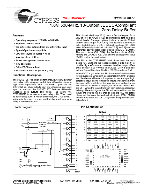
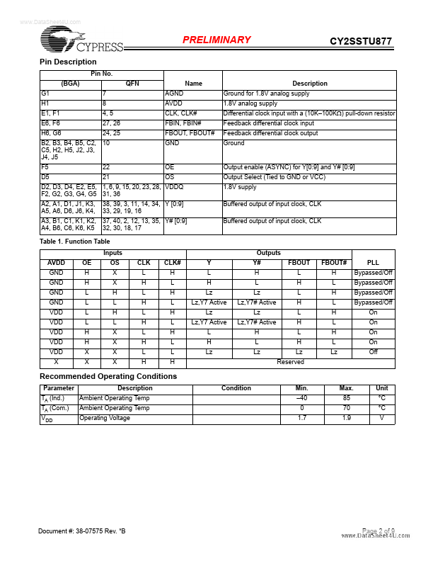
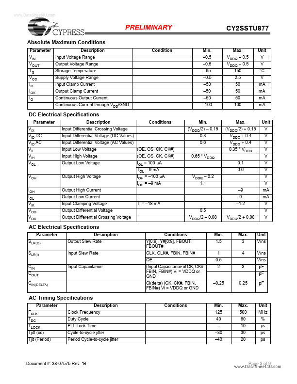
The CY2SSTU877 is a high-performance, low-skew, low-jitter zero delay buffer designed to distribute differential clocks in high-speed applications.
The CY2SSTU877 generates ten differential pair clock outputs from one differential pair clock input.
| Part number | CY2SSTU877 |
|---|---|
| Manufacturer | Cypress (Infineon) |
| File Size | 253.19 KB |
| Description | 10-Output JEDEC-Compliant Zero Delay Buffer |
| Datasheet |
CY2SSTU877 Datasheet
|
|
|
|
| Part Number | Description | Manufacturer |
|---|---|---|
| CY2SSTV16857 | 14-Bit Regstered Buffer | SpectraLinear |
| CY2SSTV16859 | 13-Bit to 26-Bit Registered Buffer | SpectraLinear |
| CY2SSTV850 | Differential Clock Buffer/Driver | Silicon Laboratories |
| CY2SSTV855 | Differential Clock Buffer/Driver | Silicon Laboratories |
| CY2SSTV857-27 | Differential Clock Buffer/Driver DDR333/PC2700-Compliant | Silicon Laboratories |
| Part Number | Description |
|---|---|
| CY2SSTV16857 | 14-Bit Registered Buffer |
| CY2SSTV16859 | 13-Bit to 26-Bit Registered Buffer PC2700-/PC3200-Compliant |
| CY2SSTV850 | Differential Clock Buffer/Driver |
| CY2SSTV855 | Differential Clock Buffer/Driver |
| CY2SSTV857-27 | Differential Clock Buffer/Driver DDR333/PC2700-Compliant |
The following content is an automatically extracted verbatim text from the original manufacturer datasheet and is provided for reference purposes only.