Click to expand full text
CY2SSTV16859
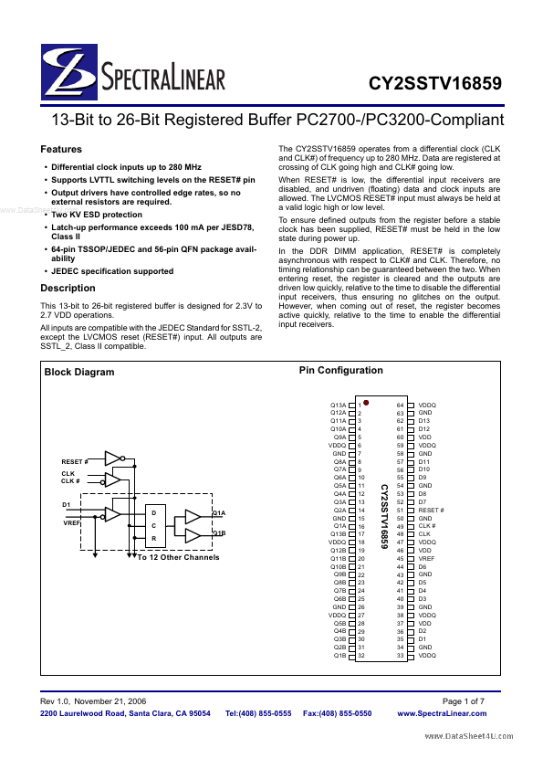
13-Bit to 26-Bit Registered Buffer PC2700-/PC3200-Compliant
Features
• Differential clock inputs up to 280 MHz • Supports LVTTL switching levels on the RESET# pin • Output drivers have controlled edge rates, so no external resistors are required.
www.DataSheet4U.com
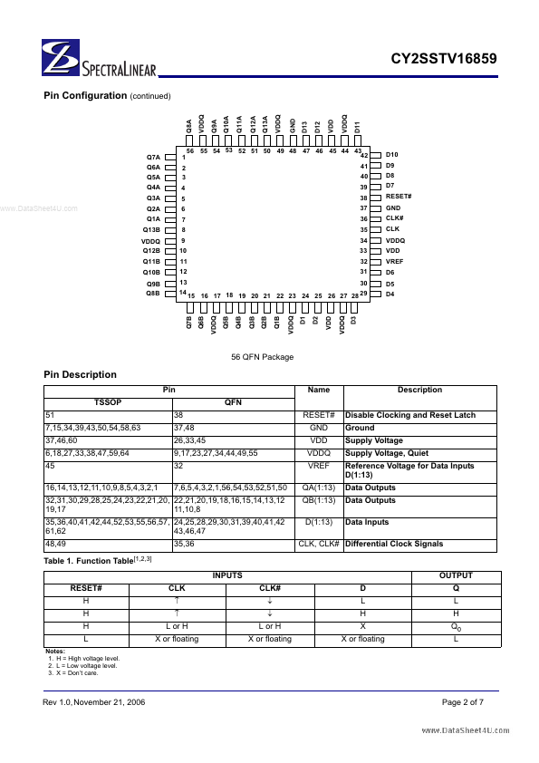
The CY2SSTV16859 operates from a differential clock (CLK and CLK#) of frequency up to 280 MHz. Data are registered at crossing of CLK going high and CLK# going low. When RESET# is low, the differential input receivers are disabled, and undriven (floating) data and clock inputs are allowed. The LVCMOS RESET# input must always be held at a valid logic high or low level. To ensure defined outputs from the register before a stable clock has been supplied, RESET# must be held in the low state during power up.
 CY2SSTV16859 Datasheet