Datasheet Details
| Part number | CY2SSTV16857 |
|---|---|
| Manufacturer | Cypress (Infineon) |
| File Size | 178.83 KB |
| Description | 14-Bit Registered Buffer |
| Datasheet |
 CY2SSTV16857 Datasheet CY2SSTV16857 Datasheet
|
|
|
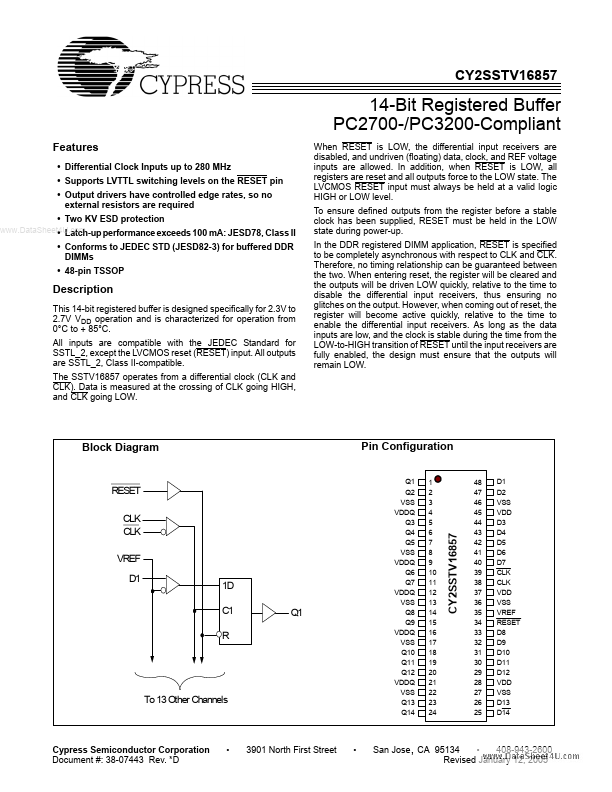
This 14-bit registered buffer is designed specifically for 2.3V to 2.7V VDD operation and is characterized for operation from 0°C to + 85°C.
All inputs are compatible with the JEDEC Standard for SSTL_2, except the LVCMOS reset (RESET) input.
All outputs are SSTL_2, Class II-compatible.
| Part number | CY2SSTV16857 |
|---|---|
| Manufacturer | Cypress (Infineon) |
| File Size | 178.83 KB |
| Description | 14-Bit Registered Buffer |
| Datasheet |
CY2SSTV16857 Datasheet
|
|
|
|
| Part Number | Description | Manufacturer |
|---|---|---|
| CY2SSTV16857 | 14-Bit Regstered Buffer | SpectraLinear |
| CY2SSTV16859 | 13-Bit to 26-Bit Registered Buffer | SpectraLinear |
| CY2SSTV850 | Differential Clock Buffer/Driver | Silicon Laboratories |
| CY2SSTV855 | Differential Clock Buffer/Driver | Silicon Laboratories |
| CY2SSTV857-27 | Differential Clock Buffer/Driver DDR333/PC2700-Compliant | Silicon Laboratories |
| Part Number | Description |
|---|---|
| CY2SSTV16859 | 13-Bit to 26-Bit Registered Buffer PC2700-/PC3200-Compliant |
| CY2SSTV850 | Differential Clock Buffer/Driver |
| CY2SSTV855 | Differential Clock Buffer/Driver |
| CY2SSTV857-27 | Differential Clock Buffer/Driver DDR333/PC2700-Compliant |
| CY2SSTV857-32 | Differential Clock Buffer/Driver DDR400/PC3200-Compliant |