Click to expand full text
CY2SSTV850
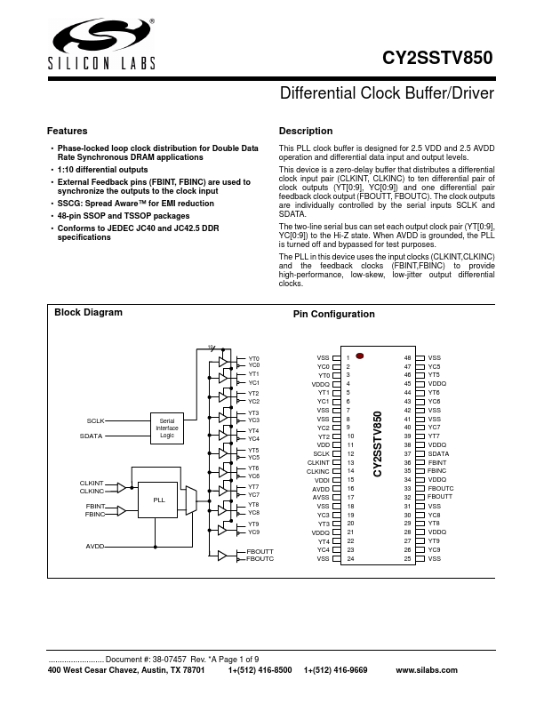
Differential Clock Buffer/Driver
Features
• Phase-locked loop clock distribution for Double Data Rate Synchronous DRAM applications
• 1:10 differential outputs • External Feedback pins (FBINT, FBINC) are used to
synchronize the outputs to the clock input • SSCG: Spread Aware™ for EMI reduction • 48-pin SSOP and TSSOP packages • Conforms to JEDEC JC40 and JC42.5 DDR
specifications
Description
This PLL clock buffer is designed for 2.5 VDD and 2.5 AVDD operation and differential data input and output levels.
This device is a zero-delay buffer that distributes a differential clock input pair (CLKINT, CLKINC) to ten differential pair of clock outputs (YT[0:9], YC[0:9]) and one differential pair feedback clock output (FBOUTT, FBOUTC).
 CY2SSTV850 Datasheet