Description
PCS3P622Z05/09 is a versatile, 3.3V Zero-delay buffer
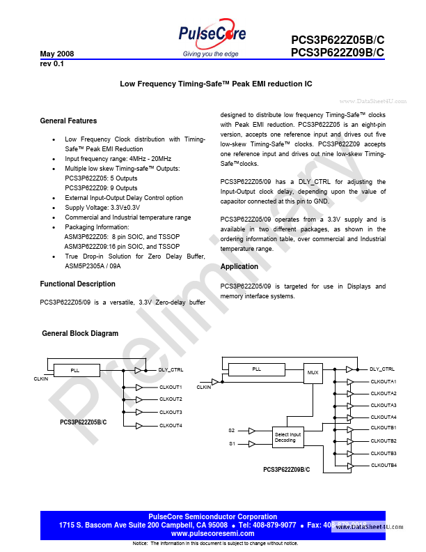
General Block Diagram
PLL CLKIN
DLY_CTRL CLKOUT1 CLKOUT2 CLKIN
PLL
MUX
DLY_CTRL CLKOUTA1 CLKOUTA2 CLKOUTA3
CLKOUT3
CLKOUTA4 S2 S1 CLKOUTB1 Select Input Decoding CLKOUTB2 CLKOUTB3
PCS3P622Z05B/C
CLKOUT4
PCS3P622Z09B/C
CLKOUTB4
PulseCore Semiconductor Corporation 1715 S.Bascom Ave Suite 200 Campbell, CA 95008
Tel: 408-879-9077
Fax: 408-879-9018 www.pulsecoresemi.com
Notice: The information in this document is s
Features
- Low Frequency Clock distribution with TimingSafe™ Peak EMI Reduction Input frequency range: 4MHz - 20MHz Multiple low skew Timing-safe™ Outputs: PCS3P622Z05: 5 Outputs PCS3P622Z09: 9 Outputs.
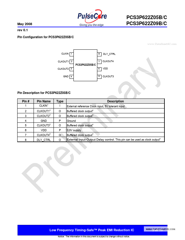
- External Input-Output Delay Control option Supply Voltage: 3.3V±0.3V Commercial and Industrial temperature range Packaging Information: ASM3P622Z05: 8 pin SOIC, and TSSOP ASM3P622Z09:16 pin SOIC, and TSSOP.
- True Drop-in Solution f.
 PCS3P622Z05B_PulseCoreSemiconductor.pdf