Description
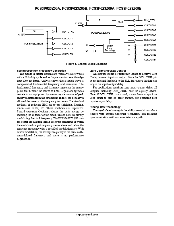
PCS3P623Z05/09 is a versatile, 3.3 V Zero
delay buffer designed
to distribute Timing
Safe clocks with Peak EMI reduction.
pin version, accepts one reference input and drives out five low
skew Timing
Safe clocks.
skew Timing
Safe clocks.
Output clock delay, depending upon the value of capacitor
Features
- Clock Distribution with Timing.
- Safe Peak EMI Reduction.
- Input Frequency Range: 20 MHz.
- 50 MHz.
- Multiple Low Skew Timing.
- Safe Outputs:
PCS3P623Z05: 5 Outputs PCS3P623Z09: 9 Outputs.
- External Input.
- Output Delay Control Option.
- Supply Voltage: 3.3 V ± 0.3 V.
- Commercial and Industrial Temperature Range.
- Packaging Information:
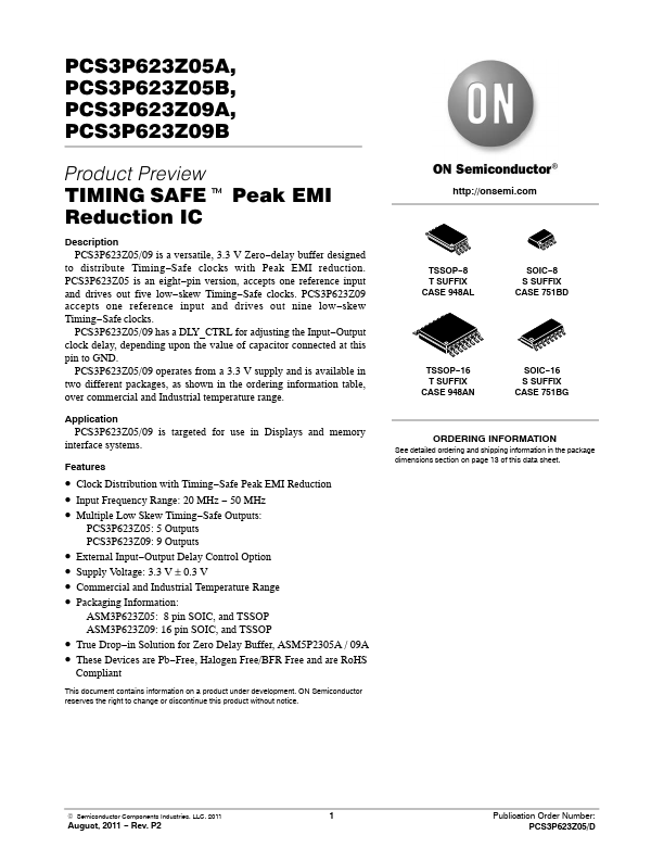
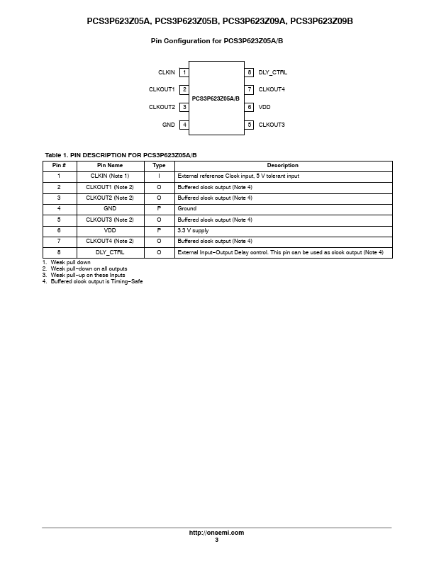
ASM3P623Z05: 8 pin SOIC, and TSSOP ASM3P623Z09: 16 pin SOIC, and TSSOP.


