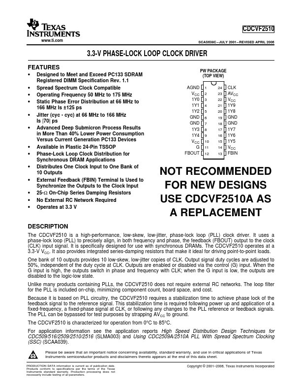
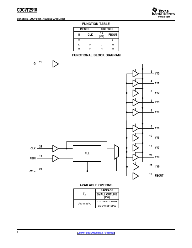
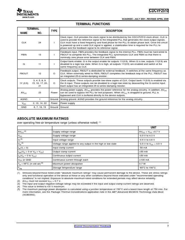
Datasheet Summary
.ti.
SCAS638C
- JULY 2001
- REVISED APRIL 2006
3.3-V PHASE-LOCK LOOP CLOCK DRIVER
Features
- Designed to Meet and Exceed PC133 SDRAM Registered DIMM Specification Rev. 1.1
- Spread Spectrum Clock patible
- Operating Frequency 50 MHz to 175 MHz
- Static Phase Error Distribution at 66 MHz to
166 MHz Is ±125 ps
- Jitter (cyc
- cyc) at 66 MHz to 166 MHz Is |70| ps
- Advanced Deep Submicron Process Results in More Than 40% Lower Power Consumption Versus Current Generation PC133 Devices
- Available in Plastic 24-Pin TSSOP
- Phase-Lock Loop Clock Distribution for
Synchronous DRAM Applications
- Distributes One Clock Input to One Bank of 10 Outputs
- External Feedback (FBIN)...