SSM5H16TU
SSM5H16TU is Silicon Epitaxial Schottky Barrier Diode manufactured by Toshiba.
Silicon N Channel MOS Type (U-MOSⅢ)/Silicon Epitaxial Schottky Barrier Diode
DC-DC Converter Applications
- -
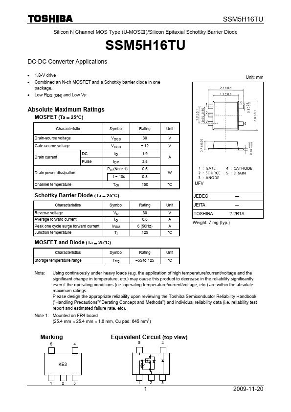
- 1.8-V drive bined an N-ch MOSFET and a Schottky barrier diode in one package. Low RDS (ON) and Low VF Unit: mm
Absolute Maximum Ratings
MOSFET (Ta = 25°C)
Characteristic Drain-source voltage Gate-source voltage Drain current DC Pulse Symbol VDSS VGSS ID IDP PD (Note 1) t = 10s Tch Rating 30 ± 12 1.9 3.8 0.5 0.8 150 Unit V V A
Drain power dissipation Channel temperature
W °C
UFV JEDEC ― ― 2-2R1A
Schottky Barrier Diode (Ta = 25°C)
Characteristics Reverse voltage Average forward current Peak one cycle surge forward current Junction temperature Symbol VR IO IFSM Tj Rating 30 0.8 6 (50Hz) 125 Unit V A A °C
JEITA TOSHIBA
Weight: 7 mg (typ.)
MOSFET and Diode (Ta = 25°C)
Characteristics Storage temperature range Symbol Tstg Rating
- 55 to 125 Unit °C
Note:
Using continuously under heavy loads (e.g. the application of high temperature/current/voltage and the significant change in temperature, etc.) may cause this product to decrease in the reliability significantly even if the operating conditions (i.e. operating temperature/current/voltage, etc.) are within the absolute maximum ratings. Please design the appropriate reliability upon reviewing the Toshiba Semiconductor Reliability Handbook (“Handling Precautions”/“Derating Concept and Methods”) and individual reliability data (i.e. reliability test report and estimated failure rate, etc).
Note 1: Mounted on FR4 board (25.4 mm × 25.4 mm × 1.6 mm, Cu pad: 645 mm2)
Marking
5 4
Equivalent Circuit (top view)
5 4
KE3
2009-11-20
MOSFET Electrical Characteristics (Ta = 25°C)
Characteristic Drain-Source breakdown voltage Drain cut-off current Gate leakage current Gate threshold voltage Forward transfer admittance Drain- source ON-resistance Input capacitance Output capacitance Reverse transfer capacitance Total gate charge Gate-source charge Gate-drain...