CM100DY-24A
Overview
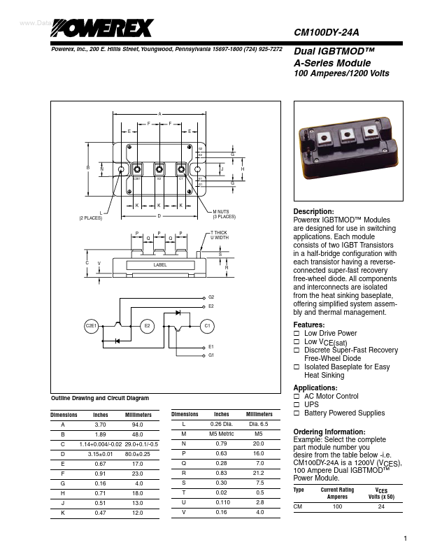
Powerex IGBTMOD™ Modules are designed for use in switching applications. Each module consists of two IGBT Transistors in a half-bridge configuration with each transistor having a reverseconnected super-fast recovery free-wheel diode.
- E F G H J K Inches 3.70 1.89 3.15±0.01 0.67 0.91 0.16 0.71 0.51 0.47 Millimeters 94.0 48.0 80.0±0.25 17.0 23.0 4.0 18.0 13.0 12.0 Dimensions L M N P Q R S T U V Inches 0.26 Dia. M5 Metric 0.79 0.63 0.28 0.83 0.30 0.02 0.110 0.16 Millimeters Dia. 6.5 M5 20.0 16.0 7.0 21.2 7.5 0.5 2.8 4.0
- 14+0.004/-0.02 29.0+0.1/-0.5 1 Powerex, Inc., 200 E. Hillis Street, Youngwood, Pennsylvania 15697-1800 (724) 925-7272 CM100DY-24A Dual IGBTMOD™ A-Series Module 100 Amperes/1200 Volts