Datasheet Details
| Part number | FDMD8630 |
|---|---|
| Manufacturer | onsemi |
| File Size | 411.09 KB |
| Description | N-Channel MOSFET |
| Datasheet |
 FDMD8630 Datasheet FDMD8630 Datasheet
|
|
|
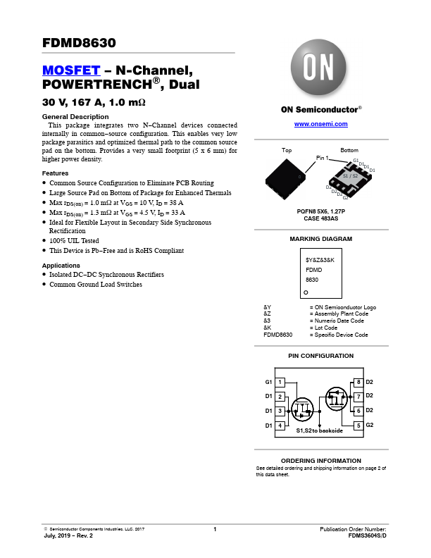
source configuration.
This enables very low package parasitics and optimized thermal path to the common source pad on the bottom.
Provides a very small footprint (5 x 6 mm) for higher power density.
| Part number | FDMD8630 |
|---|---|
| Manufacturer | onsemi |
| File Size | 411.09 KB |
| Description | N-Channel MOSFET |
| Datasheet |
FDMD8630 Datasheet
|
|
|
|
| Part Number | Description | Manufacturer |
|---|---|---|
| FDMD86100 | MOSFET | Fairchild Semiconductor |
| FDMD82100 | MOSFET | Fairchild Semiconductor |
| FDMD82100L | MOSFET | Fairchild Semiconductor |
| FDMD8280 | MOSFET | Fairchild Semiconductor |
| FDMD84100 | MOSFET | Fairchild Semiconductor |
| Part Number | Description |
|---|---|
| FDMD86100 | Dual N-Channel MOSFET |
| FDMD82100 | Dual N-Channel MOSFET |
| FDMD8430 | Dual N-Channel Power MOSFET |
| FDMD8540L | Dual N-Channel MOSFET |
| FDMD8900 | N-Channel Power MOSFET |
The following content is an automatically extracted verbatim text from the original manufacturer datasheet and is provided for reference purposes only.