The following content is an automatically extracted verbatim text
from the original manufacturer datasheet and is provided for reference purposes only.
View original datasheet text
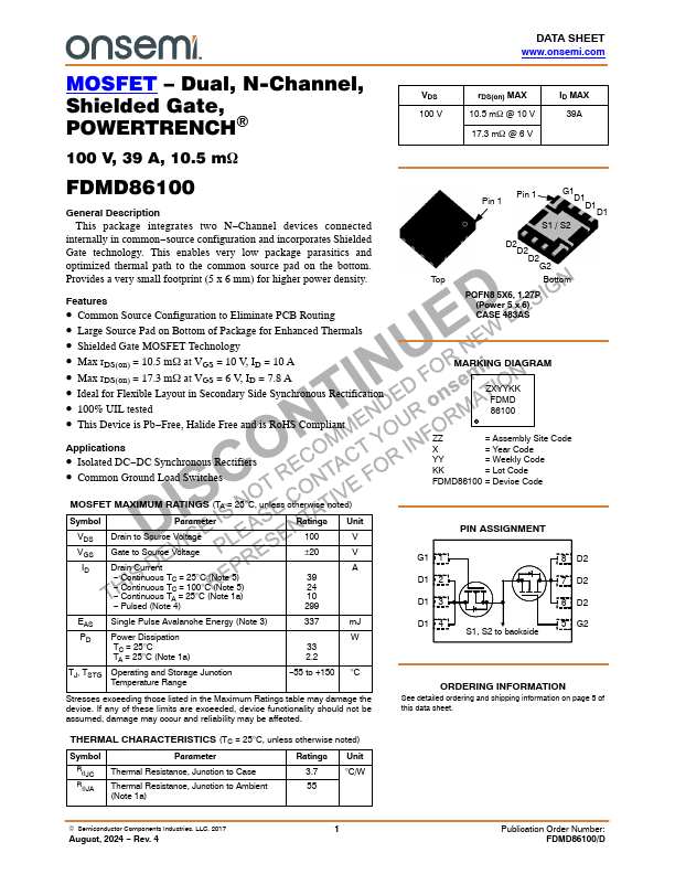
DATA SHEET www.onsemi.com
MOSFET – Dual, N-Channel, Shielded Gate, POWERTRENCH)
100 V, 39 A, 10.5 mW
VDS 100 V
rDS(on) MAX 10.5 mW @ 10 V 17.3 mW @ 6 V
ID MAX 39A
FDMD86100
General Description This package integrates two N−Channel devices connected
internally in common−source configuration and incorporates Shielded Gate technology. This enables very low package parasitics and optimized thermal path to the common source pad on the bottom. Provides a very small footprint (5 x 6 mm) for higher power density.
Features
• Common Source Configuration to Eliminate PCB Routing • Large Source Pad on Bottom of Package for Enhanced Thermals • Shielded Gate MOSFET Technology • Max rDS(on) = 10.5 mW at VGS = 10 V, ID = 10 A • Max rDS(on) = 17.3 mW at VGS = 6 V, ID = 7.
 FDMD86100 Datasheet