ICS858020
ICS858020 is LOW SKEW 1-TO-4 DIFFERENTIAL-TO-CML FANOUT BUFFER manufactured by Integrated Device Technology.
DESCRIPTION
The ICS858020 is a high speed 1-to-4 Differentialto-CML Fanout Buffer and is a member of the Hi Per Clock S™ Hi Per Clock S™ family of high performance clock solutions from ICS. The ICS858020 is optimized for high speed and very low output skew, making it suitable for use in demanding applications such as SONET, 1 Gigabit and 10 Gigabit Ethernet, and Fibre Channel. The internally terminated differential input and VREF_ AC pin allow other differential signal families such as LVDS, LVHSTL and CML to be easily interfaced to the input with minimal use of external ponents. The ICS858020 is packaged in a small 3mm x 3mm 16-pin VFQFN package which makes it ideal for use in space-constrained applications.
FEATURES
- Four differential CML outputs
- One LVPECL differential clock input
- IN, n IN pair can accept the following differential input levels: LVPECL, LVDS, CML, SSTL
- Maximum output frequency: 3.2GHz
- Output skew: 30ps (maximum)
- Part-to-part skew: 225ps (maximum)
- Additive phase jitter, RMS: <0.03ps (typical)
- Propagation delay: 600ps (maximum)
- Operating voltage supply range: VCC = 2.375V to 3.63V, VEE = 0V
- -40°C to 85°C ambient operating temperature
- Available in both standard (Ro HS5) and lead-free (Ro HS 6) packages
IC S
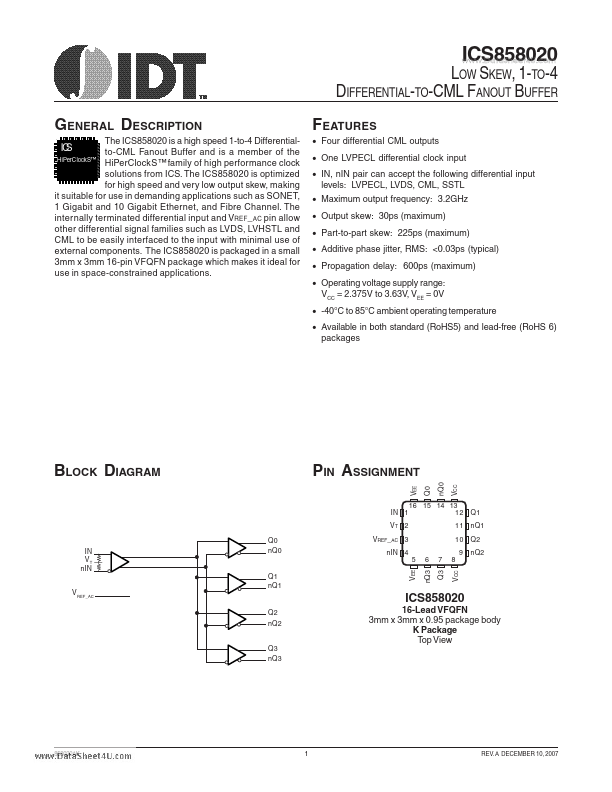
BLOCK DIAGRAM
PIN ASSIGNMENT n Q0
IN 1 VT 2 Q0 n Q0 VREF_AC 3 n IN 4
16 15 14 13 12 11 10 9 5
Q0
Q1 n Q1 Q2 n Q2 n Q3
Q1 n Q1 VREF_AC Q2 n Q2
16-Lead VFQFN 3mm x 3mm x 0.95 package body K Package Top View
Q3 n Q3
858020AK
Q3
IN VT n IN
REV. A DECEMBER 10, 2007
..
LOW SKEW, 1-TO-4 DIFFERENTIAL-TO-CML FANOUT BUFFER
TABLE 1. PIN DESCRIPTIONS
Number 1 2 3 4 5, 16 6, 7 8, 13 9, 10 11, 12 14, 15 Name IN VT VREF_AC n IN VEE n Q3, Q3 VCC n Q2, Q2 n Q1, Q1 n Q0, Q0 Input Input Output Input Power Output Power Output Output Output Type Description
Non-inver ting LVPECL differential clock input. This input internally terminates with 50Ω to the VT pin. Termination input. Reference voltage for...