Datasheet Details
| Part number | IS42SM32200M |
|---|---|
| Manufacturer | ISSI (now Infineon) |
| File Size | 856.23 KB |
| Description | 512K x 32Bits x 4Banks Mobile Synchronous DRAM |
| Datasheet |
 IS42SM32200M Datasheet IS42SM32200M Datasheet
|
|
|
Download the IS42SM32200M datasheet PDF. This datasheet also covers the IS42VM32200M variant, as both devices belong to the same 512k x 32bits x 4banks mobile synchronous dram family and are provided as variant models within a single manufacturer datasheet.
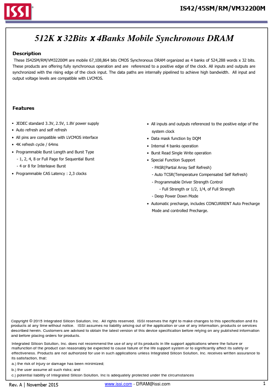
These IS42SM/RM/VM32200M are mobile 67,108,864 bits CMOS Synchronous DRAM organized as 4 banks of 524,288 words x 32 bits.
These products are offering fully synchronous operation and are referenced to a positive edge of the clock.
| Part number | IS42SM32200M |
|---|---|
| Manufacturer | ISSI (now Infineon) |
| File Size | 856.23 KB |
| Description | 512K x 32Bits x 4Banks Mobile Synchronous DRAM |
| Datasheet |
IS42SM32200M Datasheet
|
|
|
|
| Part Number | Description | Manufacturer |
|---|---|---|
| IS42S16100 | 512K Words x 16Bits x 2 Banks Synchronous Dynamic RAM | Integrated Silicon Solution |
| IS42S16100E | 512K Words x 16 Bits x 2 Banks 16Mb SYNCHRONOUS DYNAMIC RAM | Integrated Silicon Solution |
| IS42S16128 | 128K words x 16 Bits x 2 Banks SDRAM | Integrated Silicon |
| IS42S16160 | 16Meg x16 256-MBIT SYNCHRONOUS DRAM | Integrated Silicon Solution |
| IS42S16160B | 256-MBIT SYNCHRONOUS DRAM | Integrated Silicon Solution |
| Part Number | Description |
|---|---|
| IS42SM32200G | 512K x 32Bits x 4Banks Low Power Synchronous DRAM |
| IS42SM32200K | 512K x 32Bits x 4Banks Mobile Synchronous DRAM |
| IS42SM32100C | 512K x 32Bits x 2Banks Low Power Synchronous DRAM |
| IS42SM32100D | 512K x 32Bits x 2Banks Low Power Synchronous DRAM |
| IS42SM32160C | 512Mb Mobile Synchronous DRAM |
The following content is an automatically extracted verbatim text from the original manufacturer datasheet and is provided for reference purposes only.