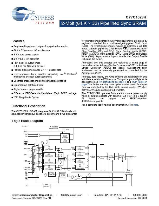
CY7C1329H
2-Mbit (64 K × 32) Pipelined Sync SRAM
Features
■ Registered inputs and outputs for pipelined operation
■ 64 K × 32 common I/O architecture
■ 3.3 V core power supply
■ 2.5 V/3.3 V I/O operation
■ Fast clock-to-output times
❐ 4.0 ns (for 133-MHz device)
■ Provide high-performance 3-1-1-1 access rate
■ User-selectable burst counter supporting Intel Pentium®
interleaved or linear burst sequences
■ Separate processor and controller address strobes
■ Synchronous self-timed write
■ Asynchronous output enable
■ Offered in JEDEC-standard lead-free 100-pin TQFP package
■ “ZZ” Sleep Mode Option
Functional Description
The CY7C1329H SRAM integrates 64 K × 32 SRAM cells with
advanced synchronous peripheral circuitry and a two-bit counter
for internal burst operation. All synchronous inputs are gated by
registers controlled by a positive-edge-triggered Clock Input
(CLK). The synchronous inputs include all addresses, all data
inputs, address-pipelining Chip Enable (CE1), depth-expansion
Chip Enables (CE2 and CE3), Burst Control inputs (ADSC,
ADSP, and ADV), Write Enables (BW[A:D] and BWE), and Global
Write (GW). Asynchronous inputs include the Output Enable
(OE) and the ZZ pin.
Addresses and chip enables are registered at rising edge of
clock when either Address Strobe Processor (ADSP) or Address
Strobe Controller (ADSC) are active. Subsequent burst
addresses can be internally generated as controlled by the
Advance pin (ADV).
Address, data inputs, and write controls are registered on-chip
to initiate a self-timed Write cycle. This part supports Byte Write
operations (see Pin Definitions on page 4 and Truth Table on
page 7 for further details). Write cycles can be one to four bytes
wide as controlled by the Byte Write control inputs. GW when
active LOW causes all bytes to be written.
The CY7C1329H operates from a +3.3 V core power supply
while all outputs operate with either a +2.5 V or +3.3 V supply.
All inputs and outputs are JEDEC-standard
JESD8-5-compatible.
For a complete list of related documentation, click here.
Logic Block Diagram
A0, A1, A
MODE
ADV
CLK
ADSC
ADSP
BWD
BWC
BWB
BWA
BWE
GW
CE1
CE2
CE3
OE
ADDRESS
REGISTER
2 A[1:0]
Q1
BURST
COUNTER
CLR AND Q0
LOGIC
DQD
BYTE
WRITE REGISTER
DQC
BYTE
WRITE REGISTER
DQB
BYTE
WRITE REGISTER
DQA
BYTE
WRITE REGISTER
ENABLE
REGISTER
PIPELINED
ENABLE
DQD
BYTE
WRITE DRIVER
DQC
BYTE
WRITE DRIVER
DQB
BYTE
WRITE DRIVER
DQA
BYTE
WRITE DRIVER
MEMORY
ARRAY
SENSE
AMPS
OUTPUT
REGISTERS
OUTPUT
BUFFERS
E
DQs
INPUT
REGISTERS
ZZ SLEEP
CONTROL
Cypress Semiconductor Corporation • 198 Champion Court
Document Number: 38-05673 Rev. *H
• San Jose, CA 95134-1709 • 408-943-2600
Revised November 20, 2014