Datasheet Details
| Part number | 74CBTLV3253D |
|---|---|
| Manufacturer | nexperia |
| File Size | 331.89 KB |
| Description | Dual 1-of-4 multiplexer/demultiplexer |
| Datasheet |
 74CBTLV3253D Datasheet 74CBTLV3253D Datasheet
|
|
|
This page provides the datasheet information for the 74CBTLV3253D, a member of the 74CBTLV3253 Dual 1-of-4 multiplexer/demultiplexer family.
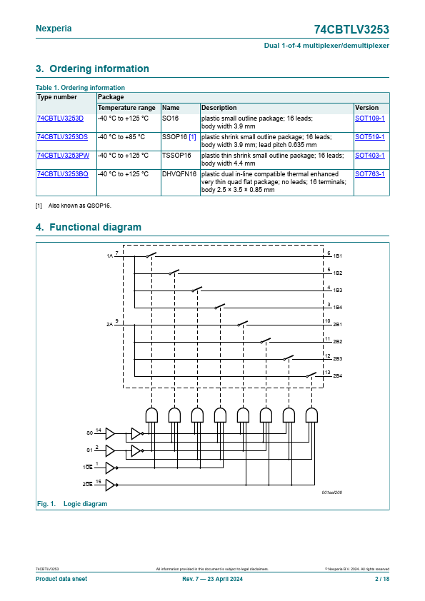
The 74CBTLV3253 provides a dual 1-of-4 high-speed multiplexer/demultiplexer with two common select inputs (S0, S1) and two output enable inputs (1OE, 2OE).

| Part number | 74CBTLV3253D |
|---|---|
| Manufacturer | nexperia |
| File Size | 331.89 KB |
| Description | Dual 1-of-4 multiplexer/demultiplexer |
| Datasheet |
74CBTLV3253D Datasheet
|
|
|
|