
SN74SSTU32864 Datasheet Text
SN74SSTU32864
25-BIT CONFIGURABLE REGISTERED BUFFER WITH SSTL_18 INPUTS AND OUTPUTS
SCES434
- MARCH 2003
D Member of the Texas Instruments
Widebus+ Family
D Pinout Optimizes DDR-II DIMM PCB Layout D Configurable as 25-Bit 1:1 or 14-Bit 1:2
Registered Buffer
D Chip-Select Inputs Gate the Data Outputs from Changing State and Minimizes System
Power Consumption
D Output Edge-Control Circuitry Minimizes
Switching Noise in an Unterminated Line
D Supports SSTL_18 Data Inputs D Differential Clock (CLK and CLK) Inputs
D Supports LVCMOS Switching Levels on the
Control and RESET Inputs
D RESET Input Disables Differential Input
Receivers, Resets All Registers, and
Forces All Outputs Low
D Latch-Up Performance Exceeds 100 mA Per
JESD 78, Class II
D ESD Protection Exceeds JESD 22
- 5000-V Human-Body Model (A114-A)
- 200-V Machine Model (A115-A)
- 1000-V Charged-Device Model (C101) description/ordering information
This 25-bit 1:1 or 14-bit 1:2 configurable registered buffer is designed for 1.7-V to 1.9-V VCC operation. In the 1:1 pinout configuration, only one device per DIMM is required to drive nine SDRAM loads. In the 1:2 pinout configuration, two devices per DIMM are required to drive 18 SDRAM loads.
All inputs are SSTL_18, except the LVCMOS reset (RESET) and LVCMOS control (Cn) inputs. All outputs are edge-controlled circuits optimized for unterminated DIMM loads and meet SSTL_18 specifications.
The SN74SSTU32864 operates from a differential clock (CLK and CLK). Data are registered at the crossing of CLK going high and CLK going low.
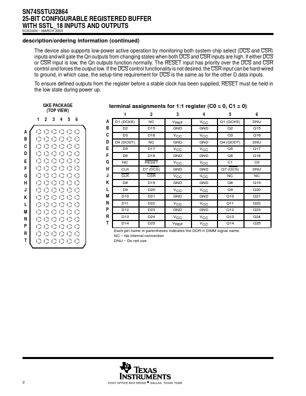
The C0 input controls the pinout configuration of the 1:2 pinout from register-A configuration (when low) to register-B configuration (when high). The C1 input controls the pinout configuration from 25-bit 1:1 (when low) to 14-bit 1:2 (when...