Datasheet Details
| Part number | SN74SSTUB32864 |
|---|---|
| Manufacturer | Texas Instruments |
| File Size | 663.57 KB |
| Description | 25-BIT CONFIGURABLE REGISTERED BUFFER |
| Datasheet |
 SN74SSTUB32864 Datasheet SN74SSTUB32864 Datasheet
|
|
|
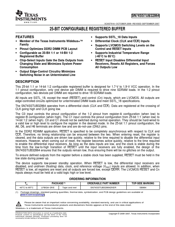
This 25-bit 1:1 or 14-bit 1:2 configurable registered buffer is designed for 1.7-V to 1.9-V VCC operation.
In the 1:1 pinout configuration, only one device per DIMM is required to drive nine SDRAM loads.
In the 1:2 pinout configuration, two devices per DIMM are required to drive 18 SDRAM loads.
| Part number | SN74SSTUB32864 |
|---|---|
| Manufacturer | Texas Instruments |
| File Size | 663.57 KB |
| Description | 25-BIT CONFIGURABLE REGISTERED BUFFER |
| Datasheet |
SN74SSTUB32864 Datasheet
|
|
|
|