Datasheet4U Logo Datasheet4U.com

SN74LVC2G07 - Dual Buffer and Driver

Description

This dual buffer and driver is designed for 1.65-V to 5.5-V VCC operation.

The output of the SN74LVC2G07 device is open drain and can be connected to other open-drain outputs to implement active-low wired-OR or active-high wired-AND functions.

The maximum sink current is 32 mA.

Features

  • 1 Dual Open-Drain Buffer Configuration.
  • -24-mA Output Drive at 3.3 V.
  • Support Translation-Up and Down.
  • Available in the Texas Instruments NanoFree™ Package.
  • Supports 5-V VCC Operation.
  • Inputs and Open-Drain Outputs Accept Voltages Up to 5.5 V.
  • Max tpd of 3.7 ns at 3.3 V.
  • Low Power Consumption, 10-μA Max ICC.
  • Typical VOLP (Output Ground Bounce).

📥 Download Datasheet

Full PDF Text Transcription

Click to expand full text
Product Folder Order Now Technical Documents Tools & Software Support & Community SN74LVC2G07 SCES308L – AUGUST 2001 – REVISED MAY 2015 
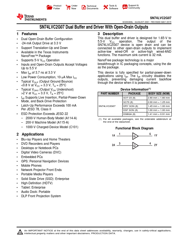
SN74LVC2G07 Dual Buffer and Driver With Open-Drain Outputs 1 Features •1 Dual Open-Drain Buffer Configuration • -24-mA Output Drive at 3.3 V • Support Translation-Up and Down • Available in the Texas Instruments NanoFree™ Package • Supports 5-V VCC Operation • Inputs and Open-Drain Outputs Accept Voltages Up to 5.5 V • Max tpd of 3.7 ns at 3.3 V • Low Power Consumption, 10-μA Max ICC • Typical VOLP (Output Ground Bounce) <0.8 V at VCC = 3.3 V, TA = 25°C • Typical VOHV (Output VOH Undershoot) >2 V at VCC = 3.
Published: |