Click to expand full text
Product Folder
Sample & Buy
Technical Documents
Tools & Software
Support & Community
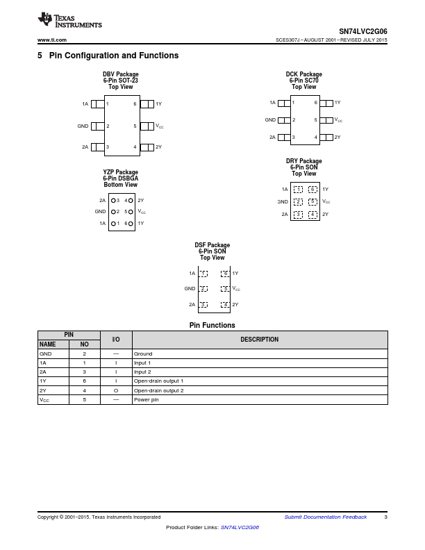
SN74LVC2G06
SCES307J – AUGUST 2001 – REVISED JULY 2015
SN74LVC2G06 Dual Inverter Buffer and Driver With Open-Drain Outputs
1 Features
•1 Available in the Texas Instruments Package
• Supports 5-V VCC Operation • Max tpd of 3.4 ns at 3.3 V • Low Power Consumption, 10-μA Max ICC • ±24-mA Output Drive at 3.3 V
• Typical VOLP (Output Ground Bounce) <0.8 V at VCC = 3.3 V, TA = 25°C
• Typical VOHV (Output VOH Undershoot) >2 V at VCC = 3.3 V, TA = 25°C
• Inputs and Open-Drain Outputs Accept Voltages up to 5.5 V
• Ioff Supports Live Insertion, Partial-Power-Down Mode and Back-Drive Protection
• Latch-Up Performance Exceeds 100 mA Per JESD 78, Class II
• Supports Down-Translation (5 V to 3.3 V and 3.3 V to 1.
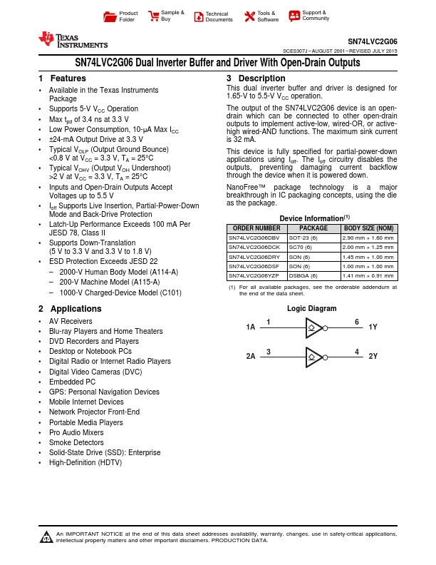
 SN74LVC2G06 Datasheet