Click to expand full text
CSD25211W1015
SLPS296A – FEBRUARY 2012 – REVISED JANUARY 2014
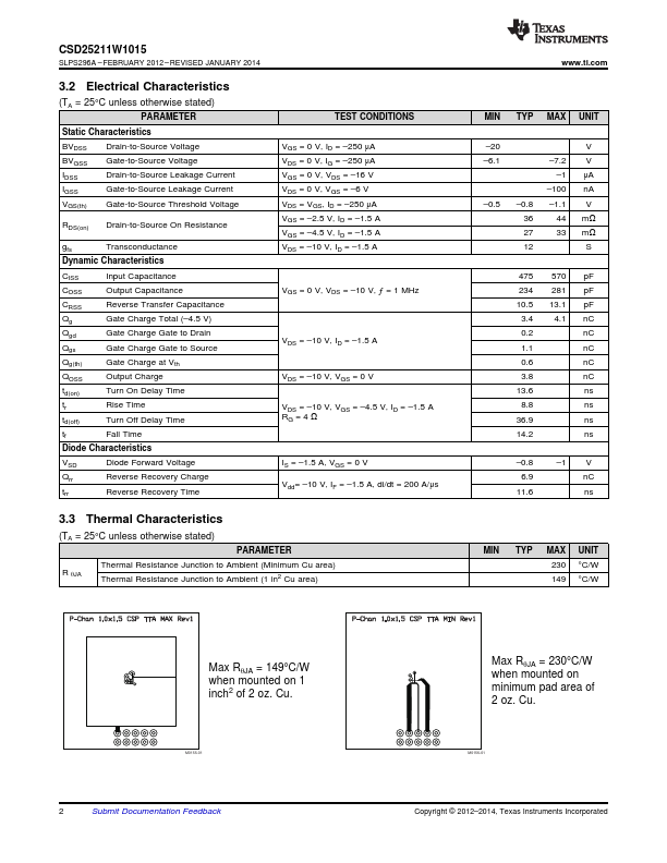
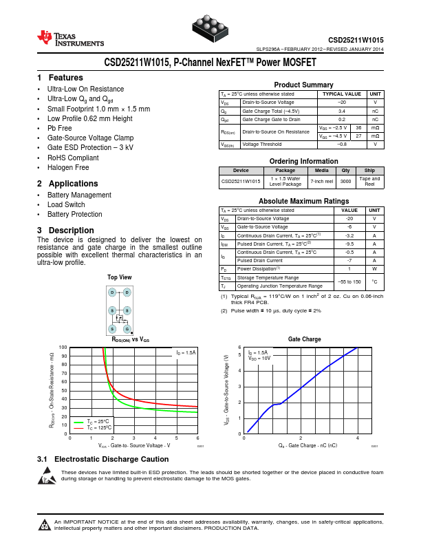
CSD25211W1015, P-Channel NexFET™ Power MOSFET
1 Features
•1 Ultra-Low On Resistance • Ultra-Low Qg and Qgd • Small Footprint 1.0 mm × 1.5 mm • Low Profile 0.62 mm Height • Pb Free • Gate-Source Voltage Clamp • Gate ESD Protection – 3 kV • RoHS Compliant • Halogen Free
2 Applications
• Battery Management • Load Switch • Battery Protection
3 Description
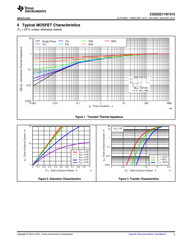
The device is designed to deliver the lowest on resistance and gate charge in the smallest outline possible with excellent thermal characteristics in an ultra-low profile.
Top View
Product Summary
TA = 25°C unless otherwise stated
VDS
Drain-to-Source Voltage
Qg
Gate Charge Total (–4.
 CSD25211W1015 Datasheet