Click to expand full text
CSD25302Q2
www.ti.com
SLPS234B – NOVEMBER 2009 – REVISED JANUARY 2012
P-Channel NexFET™ Power MOSFET
FEATURES
1
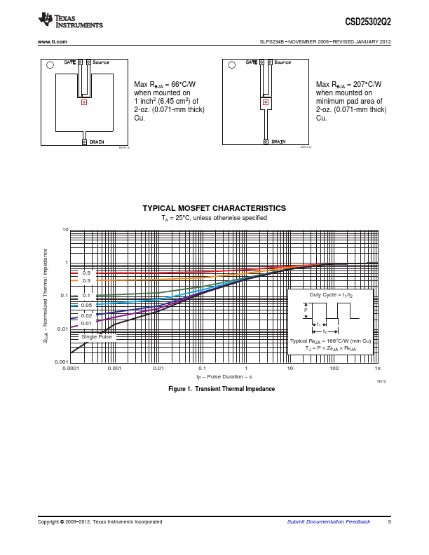
• Ultralow Qg and Qgd • Low Thermal Resistance • Avalanche Rated • Pb Free Terminal Plating • RoHS Compliant • Halogen Free • SON 2-mm × 2-mm Plastic Package
APPLICATIONS
• Battery Management • Load Management • Battery Protection
DESCRIPTION
The device has been designed to deliver the lowest on resistance and gate charge in the smallest outline possible with excellent thermal characteristics in an ultra low profile. Low on resistance coupled with the extremely small footprint and low profile make the device ideal for battery operated space constrained applications.
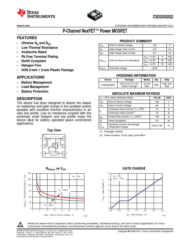
Top View
S1 S
6S
PRODUCT SUMMARY
VDS
Drain to Source Voltage
–20
V
Qg
Gate Charge Total (–4.5V)
2.
 CSD25302Q2 Datasheet