Click to expand full text
P0950ETF / P0950ETFS
N-Channel Enhancement Mode MOSFET
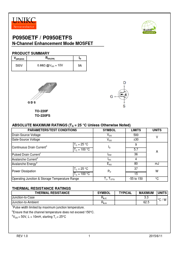
PRODUCT SUMMARY
V(BR)DSS
RDS(ON)
ID
500V
0.88Ω @VGS = 10V
9A
TO-220F TO-220FS
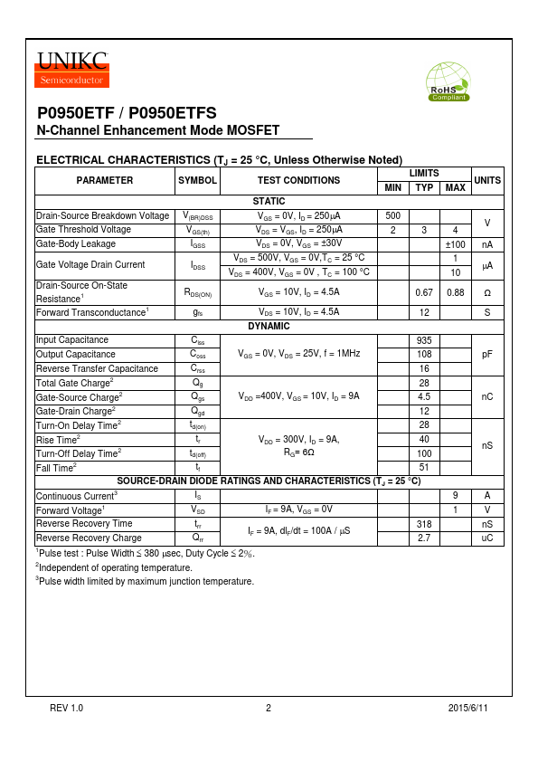
ABSOLUTE MAXIMUM RATINGS (TA = 25 °C Unless Otherwise Noted)
PARAMETERS/TEST CONDITIONS
SYMBOL
LIMITS
Drain-Source Voltage
VDS
500
Gate-Source Voltage
VGS
±30
Continuous Drain Current2
Pulsed Drain Current1 Avalanche Current3 Avalanche Energy3
TC = 25 °C TC = 100 °C
ID
9 5.7
IDM
36
IAS
4
EAS
80
Power Dissipation
TC = 25 °C
PD
37
TC = 100 °C
15
Operating Junction & Storage Temperature Range
TJ, TSTG
-55 to 150
UNITS V
A
mJ W °C
THERMAL RESISTANCE RATINGS
THERMAL RESISTANCE
Junction-to-Case
Junction-to-Ambient 1Pulse width limited by maximum junction temperature. 2Ensure that the channel temperature does not exceed 150°C.
 P0950ETFS Datasheet