Datasheet4U Logo Datasheet4U.com

SE3082G - N-Channel MOSFET

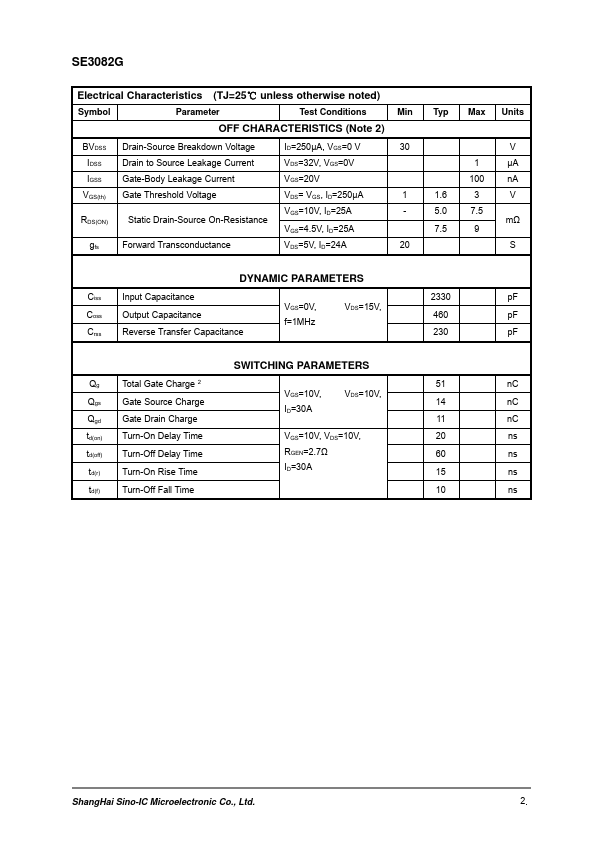
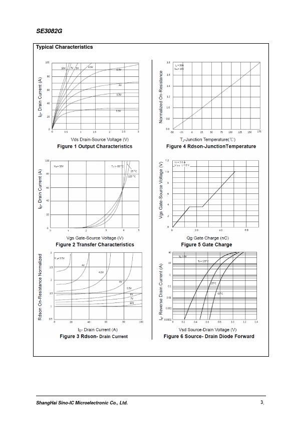
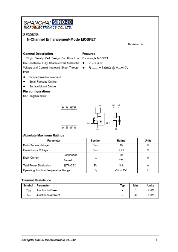
This page provides the datasheet information for the SE3082G, a member of the SE3082G-Sino N-Channel MOSFET family.

Description

Thigh Density Cell Design For Ultra Low On-Resistance Fully Characterized Avalanche Voltage and Current Improved Shoot-Through FOM Simple Drive Requirement Small Package Outline Surface Mount Device

Features

  • For a single MOSFET.
  • VDS = 30V.
  • RDS(ON) = 5.0mΩ @ VGS=10V Pin configurations See Diagram below D1 D1 D2 S1D2 87 65 D1 D1 D2 D2 1 2 34 G1 S2 S2 G2 Absolute Maximum Ratings Parameter Drain-Source Voltage Gate-Source Voltage Drain Current Continuous Pulsed Total Power Dissipation @TA=25℃ Operating Junction Temperature Range Thermal Resistance Symbol RθJC RθJA Parameter Junction to Case Junction to Ambient G1 S1 G2 S2 Symbol VDS VGS ID PD TJ Rating 30 ±20 80 170 3.1 -5.

📥 Download Datasheet

Datasheet preview – SE3082G

Datasheet Details

Part number SE3082G
Manufacturer Sino-IC
File Size 590.23 KB
Description N-Channel MOSFET
Datasheet download datasheet SE3082G Datasheet
Additional preview pages of the SE3082G datasheet.
Other Datasheets by Sino-IC

Full PDF Text Transcription

Click to expand full text
SE3082G N-Channel Enhancement-Mode MOSFET Revision: A General Description Thigh Density Cell Design For Ultra Low On-Resistance Fully Characterized Avalanche Voltage and Current Improved Shoot-Through FOM  Simple Drive Requirement  Small Package Outline  Surface Mount Device Features For a single MOSFET  VDS = 30V  RDS(ON) = 5.0mΩ @ VGS=10V Pin configurations See Diagram below D1 D1 D2 S1D2 87 65 D1 D1 D2 D2 1 2 34 G1 S2 S2 G2 Absolute Maximum Ratings Parameter Drain-Source Voltage Gate-Source Voltage Drain Current Continuous Pulsed Total Power Dissipation @TA=25℃ Operating Junction Temperature Range Thermal Resistance Symbol RθJC RθJA Parameter Junction to Case Junction to Ambient G1 S1 G2 S2 Symbol VDS VGS ID PD TJ Rating 30 ±20 80 170 3.
Published: |