Click to expand full text
www.DataSheet4U.com
16 MBit Synchronous DRAM
HYB 39S16400/800/160CT-8/-10
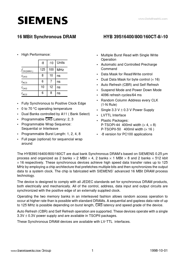
• High Performance:
-8 -10 100 10 7 12 8
Units MHz ns ns ns ns
fCK(MAX.) tCK3 tAC3 tCK2 tAC2
125 8 6 10 6
• Multiple Burst Read with Single Write Operation • Automatic and Controlled Precharge Command • Data Mask for Read/Write control • Dual Data Mask for byte control (× 16) • Auto Refresh (CBR) and Self Refresh • Suspend Mode and Power Down Mode • 4096 refresh cycles/64 ms • Random Column Address every CLK (1-N Rule) • Single 3.3 V ± 0.
 HYB39S16160CT-8 Datasheet