Click to expand full text
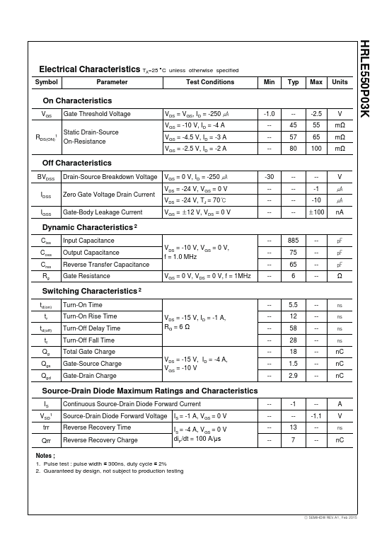
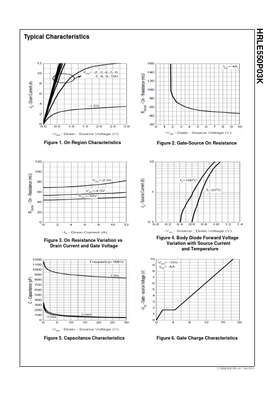
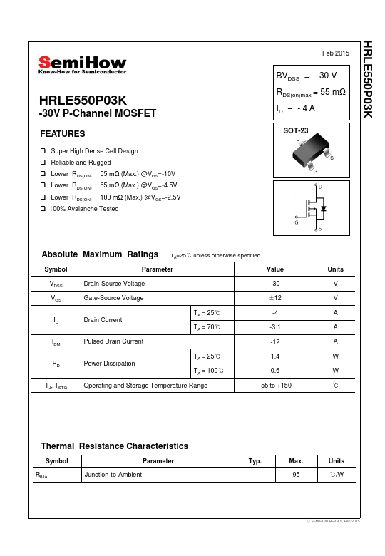
HRLE550P03K
HRLE550P03K
-30V P-Channel MOSFET
FEATURES
Super High Dense Cell Design Reliable and Rugged Lower RDS(ON) : 55 Pȍ (Max.) @VGS=-10V Lower RDS(ON) : 65 Pȍ (Max.) @VGS=-4.5V Lower RDS(ON) : 100 Pȍ (Max.) @VGS=-2.5V 100% Avalanche Tested
Feb 2015
BVDSS = - 30 V RDS(on)max = 55 Pȍ ID = - 4 A
SOT-23
D
S G
Absolute Maximum Ratings TA=25 unless otherwise specified
Symbol
Parameter
Value
VDSS VGS ID IDM PD TJ, TSTG
Drain-Source Voltage
Gate-Source Voltage
Drain Current Pulsed Drain Current
TA = 25 TA = 70
Power Dissipation
TA = 25 TA = 100
Operating and Storage Temperature Range
-30 ρ12
-4 -3.1 -12 1.4 0.6 -55 to +150
Units V V A A A W W
Thermal Resistance Characteristics
Symbol
Parameter
RșJA Junction-to-Ambient
Typ. --
Max.
 HRLE550P03K Datasheet