Datasheet4U Logo Datasheet4U.com

S5T8809 - PLL FREQUENCY SYNTHESIZER FOR PAGER

Description

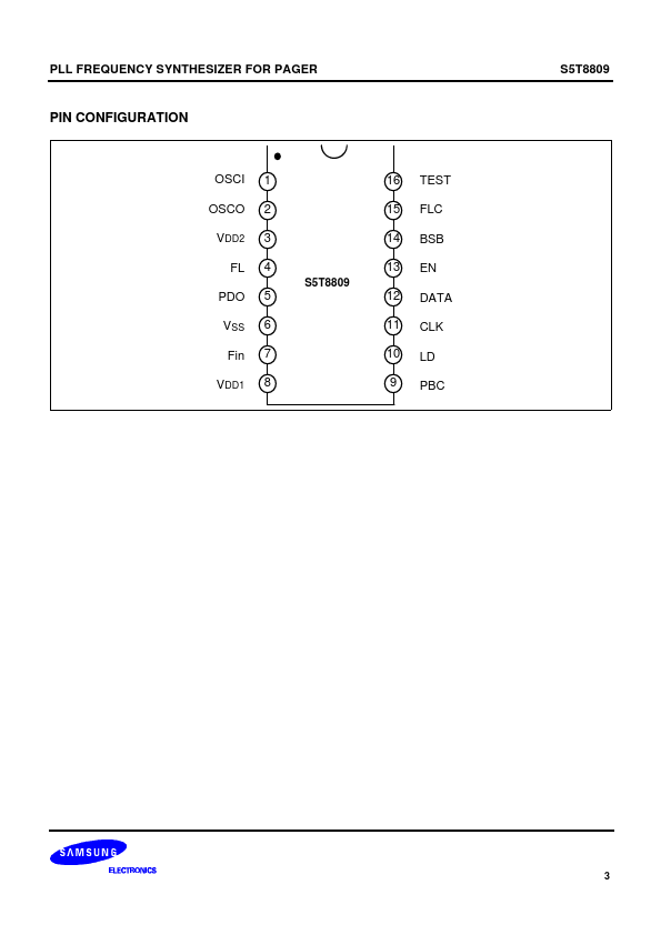
Pin No 1 2 3 4 5 6 7 8 9 Symbol OSCI OSCO VDD2 FL PDO VSS Fin VDD1 PBC Description These input / output pins generate the reference frequency.

In case of OSCI Pin, external reference frequency can be used through the AC coupling.

Features

  • Maximum operating frequency: 330MHz @ 300mVP-P, VDD1 = 1.0V, VDD2 = 3.0V On-chip reference oscillator supports external crystal which oscillates up to 23MHz Superior supply current:.
  • FFIN = 310MHz, IDD1 = 0.8mA (Typ. ) @ VDD1 = 1.0V, VDD2 = 3.0V Operating voltage: VDD1 = 0.95 to 1.5V and VDD2 = 2.0 to 3.3V Excellent Divider range:.
  • Ref. Divider: FRC (0): 1 / 40 to 1 / 65528 (Multiple): Default FRC (1): 1 / 5 to 1 / 32767.
  • Rx Divider: PBC (0.

📥 Download Datasheet

Full PDF Text Transcription (Reference)

The following content is an automatically extracted verbatim text from the original manufacturer datasheet and is provided for reference purposes only.

View original datasheet text
PLL FREQUENCY SYNTHESIZER FOR PAGER S5T8809 INTRODUCTION S5T8809 is a superior low-power-programmable PLL frequency synthesizer which can be used in high performance / Simple application for a Wide Area Pager system. S5T8809 consists of 2 kinds of divider block including a 19-bit Shift register, 16/18-bit Latch, 13/15bits R-counter and 16/18-bit NCounter, 32/33 Prescaler, and a phase detector block including a Phase detector, Lock detector and a Charge pump. S5T8809 also has a battery saving mode which can control each register block by serial control data from the µ-controller (MICOM) and it also has boost up signal output for fast locking. 16-TSSOP-0044 ( Magnification = 1 : 4 ) FEATURES • • • Maximum operating frequency: 330MHz @ 300mVP-P, VDD1 = 1.0V, VDD2 = 3.
Published: |