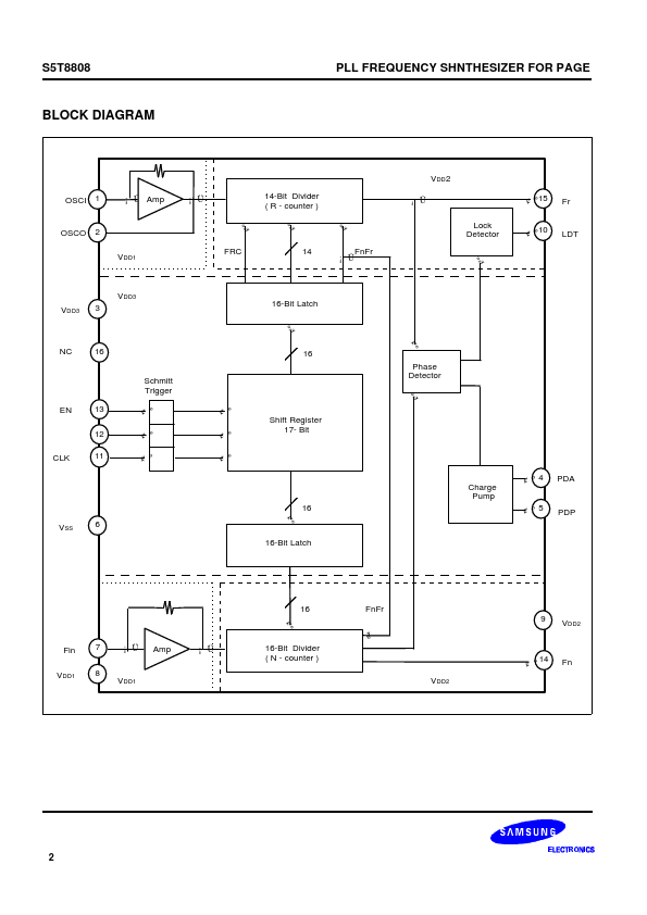
Datasheet4U Logo Datasheet4U.com

S5T8808 - PLL FREQUENCY SHNTHESIZER FOR PAGER

Description

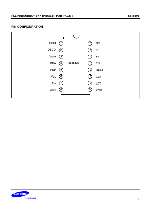
Pin No 1 2 3 4 Symbol OSCI OSCO VDD3 PDA I/O I O

O Description These input / output pins generate the reference frequency.

In case of an OSCI pin, external reference frequency can be input through an AC coupling.

Features

  • Maximum operating frequency: 150MHz @ 500mVP-P, VDD1 = 0.95V 180MHz @ 500mVP-P, VDD1 = 1.0V (Magnification = 1 : 4).
  • On-chip reference oscillator supports external crystal which oscillates up to 18MHz Superior supply current: (VDD1 = VDD2 = 1.0V, VDD3 = 3.0V).
  • FFIN = 90MHz, IDD1 = 0.6mA (Typ. ).
  • FFIN = 150MHz, IDD1 = 0.9mA (Typ. ).
  • FFIN = 180MHz, IDD3 = 1.1mA (TyP. ).
  • Operating voltage: VDD1 = 0.95 ~.

📥 Download Datasheet

Full PDF Text Transcription (Reference)

The following content is an automatically extracted verbatim text from the original manufacturer datasheet and is provided for reference purposes only.

View original datasheet text
PLL FREQUENCY SHNTHESIZER FOR PAGER S5T8808 INTRODUCTION S5T8808 is a superior low-power-programmable PLL frequency synthesizer which can be used in a high performance Wide Area Pager system. KS8808 consists of 2 kinds of divider block including a 17-bit Shift register, 16-bit Latch, 14/16-bits Counter, Prescaler, and a phase detector block including a Phase detector, Lock detector and a Charge pump. 16−SSOP−0044 FEATURES • Maximum operating frequency: 150MHz @ 500mVP-P, VDD1 = 0.95V 180MHz @ 500mVP-P, VDD1 = 1.0V (Magnification = 1 : 4) • • On-chip reference oscillator supports external crystal which oscillates up to 18MHz Superior supply current: (VDD1 = VDD2 = 1.0V, VDD3 = 3.0V) — FFIN = 90MHz, IDD1 = 0.6mA (Typ.) — FFIN = 150MHz, IDD1 = 0.9mA (Typ.) — FFIN = 180MHz, IDD3 = 1.
Published: |