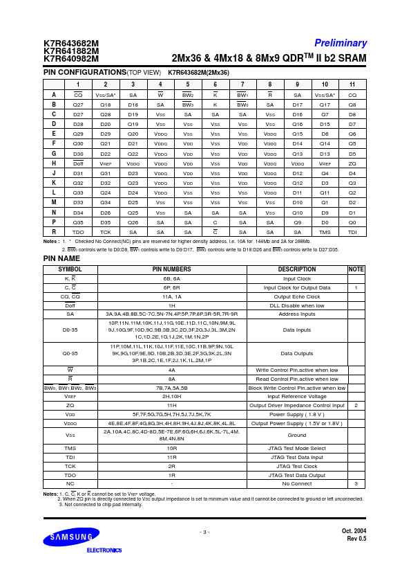
Input Clock Input Clock for Output Data Output Echo Clock DLL Disable when low Address Inputs Data Inputs 1 NOTE
Q0-35 W R BW0, BW1,BW2, BW3 VREF ZQ VDD VDDQ VSS TMS TDI TCK TDO NC
Data Outputs Write Control Pin,active when low Read Control Pin,active when low Block Write Control Pin,active when l
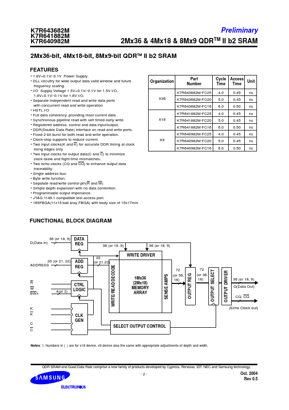
Key Features
1.8V+0.1V/-0.1V Power Supply.
DLL circuitry for wide output data valid window and future freguency scaling.
I/O Supply Voltage 1.5V+0.1V/-0.1V for 1.5V I/O, 1.8V+0.1V/-0.1V for 1.8V I/O.
Separate independent read and write data ports with concurrent read and write operation.
HSTL I/O.
Full data coherency, providing most current data.
Synchronous pipeline read with self timed early write.
Full PDF Text Transcription for K7R643682M (Reference)
Note: Below is a high-fidelity text extraction (approx. 800 characters) for
K7R643682M. For precise diagrams, and layout, please refer to the original PDF.
K7R643682M K7R641882M K7R640982M Document Title Preliminary 2Mx36 & 4Mx18 & 8Mx9 QDRTM II b2 SRAM 2Mx36-bit, 4Mx18-bit, 8Mx9-bit QDRTM II b2 SRAM Revision History Rev. No...
View more extracted text
x36-bit, 4Mx18-bit, 8Mx9-bit QDRTM II b2 SRAM Revision History Rev. No. 0.0 0.1 History 1. Initial document. 1. Update AC timing characteristics. 2. Change the JTAG instruction coding. 1. Change the AC timing characteristics. (-25/-20 parts) 2. Correct the overshoot and undershoot timing diagrams. 3. Change the JTAG Block diagrams. 4. Update the Boundary scan exit order. 1. Correct the JTAG ID register definition 2. Correct the AC timing parameter (delete the tKHKH Max value) 1. Add the Power-on Sequence specification 1. Correct the pin name table Draft Date Sep, 14 2002 Oct. 24, 2002 Remark Advance Preliminary 0.2 Feb. 18
 K7R643682M Datasheet