Input Clock Input Clock for Output Data Output Echo Clock DLL Disable when low Address Inputs Data Inputs 1 NOTE
Q0-35 W R BW0, BW1,BW2, BW3 VREF ZQ VDD VDDQ VSS TMS TDI TCK TDO NC
Data Outputs Write Control Pin, active when low Read Control Pin, active when low Block Write Control Pin, active whe
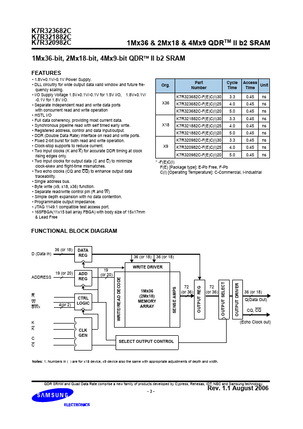
Key Features
1.8V+0.1V/-0.1V Power Supply.
DLL circuitry for wide output data valid window and future frequency scaling.
I/O Supply Voltage 1.5V+0.1V/-0.1V for 1.5V I/O, 1.8V+0.1V/ -0.1V for 1.8V I/O.
Separate independent read and write data ports with concurrent read and write operation.
HSTL I/O.
Full data coherency, providing most current data.
Synchronous pipeline read with self timed early write.
Full PDF Text Transcription for K7R320982C (Reference)
Note: Below is a high-fidelity text extraction (approx. 800 characters) for
K7R320982C. For precise diagrams, and layout, please refer to the original PDF.
I SRAM Specification 165 FBGA with Pb & Pb-Free (RoHS compliant) INFORMATION IN THIS DOCUMENT IS PROVIDED IN RELATION TO SAMSUNG PRODUCTS, AND IS SUBJECT TO CHANGE WITHOUT NOTICE. NOTHING IN THIS DOCUMENT SHALL BE CONSTRUED AS GRANTING ANY LICENSE, EXPRESS OR IMPLIED, BY ESTOPPEL OR OTHERWISE, TO ANY INTELLECTUAL PROPERTY RIGHTS IN SAMSUNG PRODUCTS OR TECHNOLOGY. ALL INFORMATION IN THIS DOCUMENT IS PROVIDED ON AS "AS IS" BASIS WITHOUT GUARANTEE OR WARRANTY OF ANY KIND. 1. For updates or additional information about Samsung products, contact your nearest Samsung office. 2.
 K7R320982C Datasheet