Built-in fast recovery diode
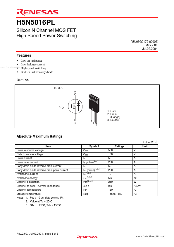
Outline
TO-3PL
D
G
S
1
1. Gate 2. Drain (Flange) 3. Source
2 3
Absolute Maximum Ratings
(Ta = 25°C)
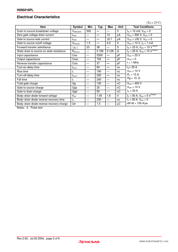
Item Drain to source voltage Gate to source voltage Drain current Drain peak current Body-drain diode reverse drain current Body-drain diode reverse drain peak current Avalanche current Avalanche energy Channel dissipation Channel to case Thermal.
H5N5012P- Silicon N Channel MOS FET High Speed Power Switching
H5N1503P- Silicon N Channel MOS FET High Speed Power Switching
H5N1506P- Silicon N Channel MOS FET High Speed Power Switching
H5N2001LD- Silicon N Channel MOS FET High Speed Power Switching
H5N2001LM- Silicon N Channel MOS FET High Speed Power Switching
H5N2001LS- Silicon N Channel MOS FET High Speed Power Switching
H5N2003P- Silicon N Channel MOS FET High Speed Power Switching
H5N2004DL- Silicon N Channel MOS FET High Speed Power Switching
Full PDF Text Transcription
Click to expand full text
H5N5016PL
Silicon N Channel MOS FET High Speed Power Switching
REJ03G0175-0200Z Rev.2.00 Jul.02.2004
Features
• Low on-resistance • Low leakage current www.DataSheet4U.com • High speed switching • Built-in fast recovery diode
Outline
TO-3PL
D
G
S
1
1. Gate 2. Drain (Flange) 3. Source
2 3
Absolute Maximum Ratings
(Ta = 25°C)
Item Drain to source voltage Gate to source voltage Drain current Drain peak current Body-drain diode reverse drain current Body-drain diode reverse drain peak current Avalanche current Avalanche energy Channel dissipation Channel to case Thermal Impedance Channel temperature Storage temperature Notes 1. PW ≤ 10 µs, duty cycle ≤ 1% 2. Value at Tc = 25°C 3.
 H5N5016PL Datasheet