The following content is an automatically extracted verbatim text
from the original manufacturer datasheet and is provided for reference purposes only.
View original datasheet text
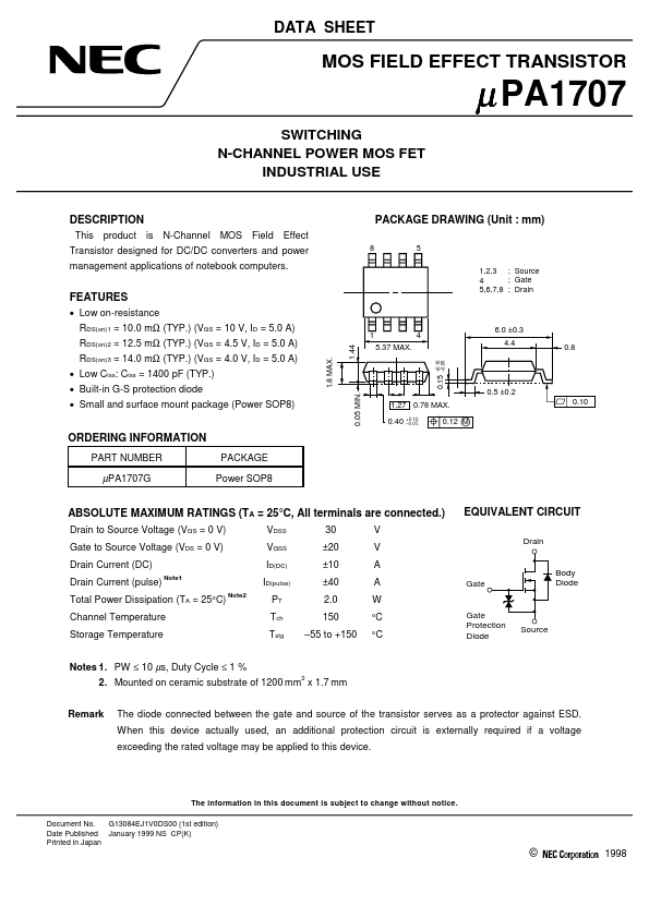
DATA SHEET
MOS FIELD EFFECT TRANSISTOR
µ PA1707
SWITCHING N-CHANNEL POWER MOS FET INDUSTRIAL USE
PACKAGE DRAWING (Unit : mm)
is N-Channel MOS Field Effect
8 5 1,2,3 ; Source ; Gate 4 5,6,7,8 ; Drain
DESCRIPTION
This product Transistor designed for DC/DC converters and power management applications of notebook computers.
FEATURES
• Low on-resistance RDS(on)1 = 10.0 mΩ (TYP.) (VGS = 10 V, ID = 5.0 A)
1.44
RDS(on)2 = 12.5 mΩ (TYP.) (VGS = 4.5 V, ID = 5.0 A)
1.8 MAX.
1 5.37 MAX.
4
6.0 ±0.3 4.4
+0.10 –0.05
0.8
RDS(on)3 = 14.0 mΩ (TYP.) (VGS = 4.0 V, ID = 5.0 A) • Low Ciss: Ciss = 1400 pF (TYP.) • Built-in G-S protection diode • Small and surface mount package (Power SOP8)
0.15
0.05 MIN.
0.5 ±0.2 0.10
1.27 0.78 MAX. 0.40
+0.10 –0.05
0.
 UPA1707 Datasheet