2N7000
MOTOROLA
SEMICONDUCTOR TECHNICAL DATA
Order this document by 2N7000/D
TMOS FET Transistor
N- Channel
- Enhancement
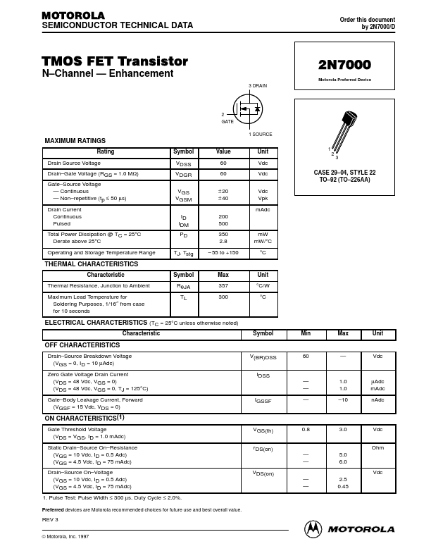
3 DRAIN 2 GATE 1 SOURCE
Motorola Preferred Device
MAXIMUM RATINGS
Rating Drain Source Voltage Drain- Gate Voltage (RGS = 1.0 MΩ) Gate- Source Voltage
- Continuous
- Non- repetitive (tp ≤ 50 µs) Drain Current Continuous Pulsed Total Power Dissipation @ TC = 25°C Derate above 25°C Operating and Storage Temperature Range Symbol VDSS VDGR VGS VGSM ID IDM PD TJ, Tstg Value 60 60 ± 20 ± 40 200 500 350 2.8
- 55 to +150 m W m W/°C °C Unit Vdc Vdc Vdc Vpk m Adc CASE 29- 04, STYLE 22 TO- 92 (TO- 226AA)
1 2 3
THERMAL CHARACTERISTICS
Characteristic Thermal Resistance, Junction to Ambient Maximum Lead Temperature for Soldering Purposes, 1/16″ from case for 10 seconds Symbol RθJA TL Max 357 300 Unit °C/W °C
ELECTRICAL CHARACTERISTICS (TC = 25°C unless otherwise noted)
Characteristic Symbol Min Max Unit
OFF CHARACTERISTICS
Drain- Source Breakdown Voltage (VGS = 0, ID = 10 µAdc) Zero...

Representative 2N7000 image (package may vary by manufacturer)