Absolute Maximum Ratings Ta = 25℃
Parameter Drain-Source Voltage
Gate-Source Voltage
Continuous Drain Current Pulsed Drain Current
Ta = 25℃ Ta = 75℃
Power Dissipation
Ta = 25℃ Ta = 75℃
Thermal Resistance. Junction- to-Ambient
Thermal Resistance. Junction- to-Fo.
The following content is an automatically extracted verbatim text
from the original manufacturer datasheet and is provided for reference purposes only.
View original datasheet text
SMD Type
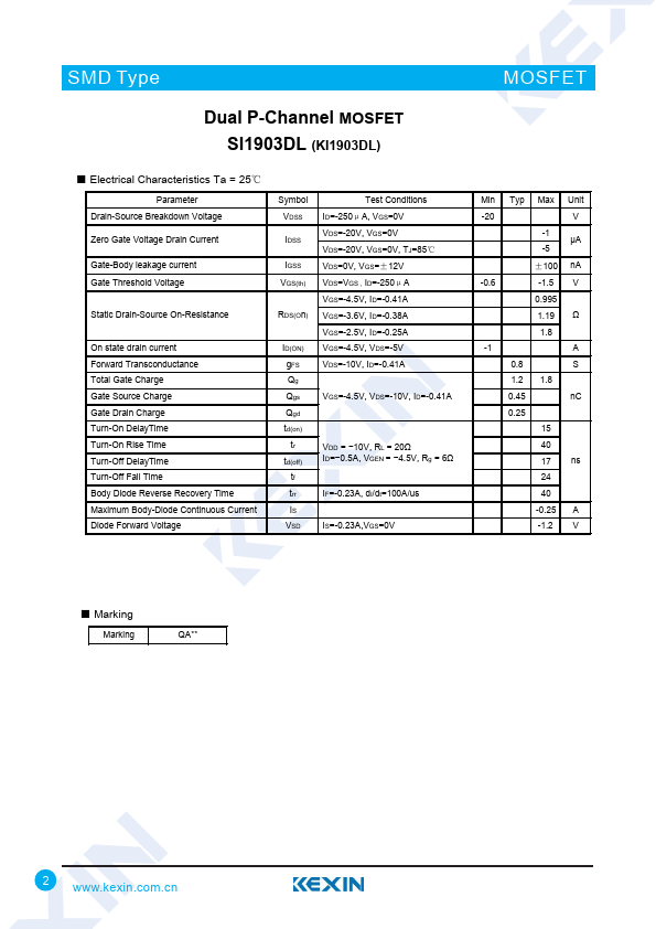
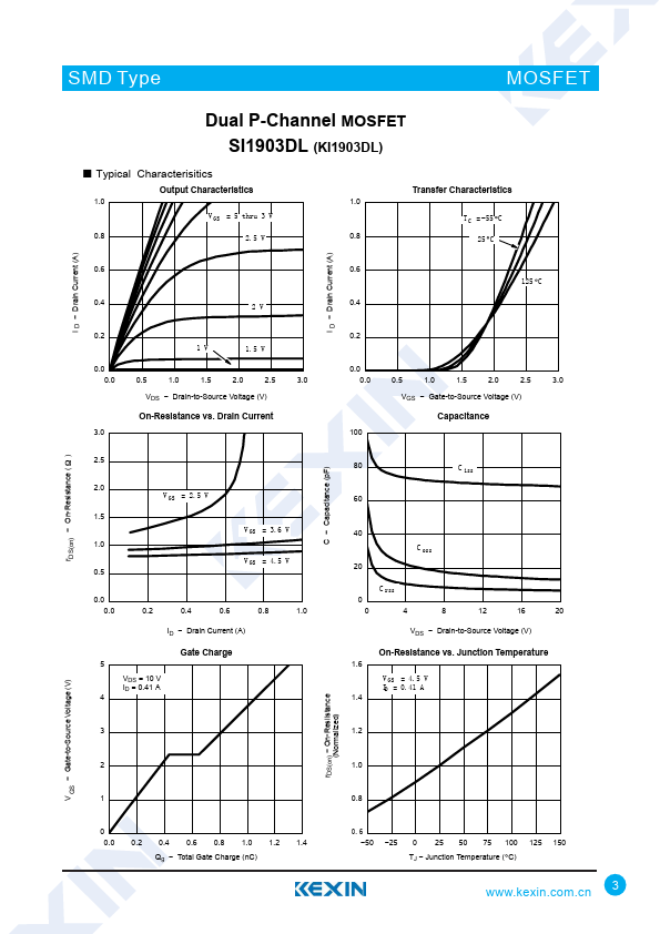
Dual P-Channel MOSFET SI1903DL (KI1903DL)
■ Features
● VDS (V) =-20V ● ID =-4.1 A (VGS =-10V) ● RDS(ON) < 0.995Ω (VGS =-4.5V) ● RDS(ON) < 1.19Ω (VGS =-3.6V) ● RDS(ON) < 1.8Ω (VGS =-2.5V)
S1 1 G1 2 D2 3
6 D1 5 G2 4 S2
MOSFET
1 S1 4 S2 2 G1 5 G2 3 D2 6 D1
■ Absolute Maximum Ratings Ta = 25℃
Parameter Drain-Source Voltage
Gate-Source Voltage
Continuous Drain Current Pulsed Drain Current
Ta = 25℃ Ta = 75℃
Power Dissipation
Ta = 25℃ Ta = 75℃
Thermal Resistance.Junction- to-Ambient
Thermal Resistance.Junction- to-Foot
Junction Temperature
Junction Storage Temperature Range
Symbol VDS VGS
ID
IDM
PD
RthJA RthJF
TJ Tstg
5 Secs
Steady State
-20
±12
- 0.44
- 0.41
- 0.31
- 0.3
-1
0.3
0.27
0.16
0.14
415
460
-
350
150
-55 to 150
Unit V
A
W ℃/W
℃
www.kexin.

 SI1903DL Datasheet