The following content is an automatically extracted verbatim text
from the original manufacturer datasheet and is provided for reference purposes only.
View original datasheet text
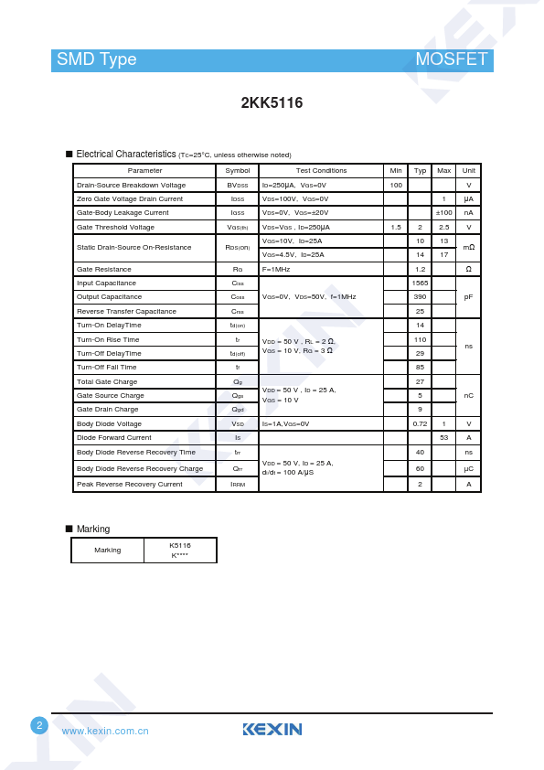
SMD Type
■ Features
● VDSS = 100V ● ID = 53A ● RDS(ON) < 13mΩ @ VGS=10V ● RDS(ON) < 17mΩ @ VGS=4.5V ● Low RDS(ON) ● 100% UIS Tested
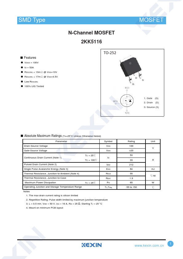
N-Channel MOSFET 2KK5116
TO-252
MOSFET
D S
G 1. Gate (G) 2. Drain (D) 3. Source (S)
■ Absolute Maximum Ratings (TA=25°C Unless Otherwise Noted)
Drain-Source Voltage Gate-Source Voltage
Parameter
Symbol VDS VGS
Continuous Drain Current (Note 1)
TC = 25℃ ID
TC = 100℃
Pulsed Drain Current (Note 2)
IDM
Single Pulse Avalanche Energy (Note 3)
EAS
Thermal Resistance, Junction-to-Ambient (Note 4)
RθJA
Thermal Resistance, Junction-to-Case
RθJC
Maximum Power Dissipation
TC = 25℃
PD
Operating Junction and Storage Temperature Range
TJ,Tstg
Notes
1. The max drain current rating is silicon limited
2.
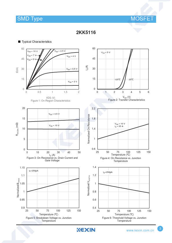
 2KK5116 Datasheet