Datasheet4U Logo Datasheet4U.com

IS61NVVP51236 - (IS61NVVP25672 / IS61NVVP51236) STATE BUS SRAM

This page provides the datasheet information for the IS61NVVP51236, a member of the IS61NVVP25672 (IS61NVVP25672 / IS61NVVP51236) STATE BUS SRAM family.

Datasheet Summary

Description

® Byte Write Control Single R/W (Read/Write) control pin Clock controlled, registered address, data and control Interleaved or linear burst sequence control using MODE input Power Down mode Common data inputs and data outputs CKE pin to

Features

  • 100 percent bus utilization.
  • No wait cycles between Read and Write.
  • Internal self-timed write cycle www. DataSheet4U. com.
  • Individual ISSI.

📥 Download Datasheet

Datasheet preview – IS61NVVP51236

Datasheet Details

Part number IS61NVVP51236
Manufacturer ISSI
File Size 215.40 KB
Description (IS61NVVP25672 / IS61NVVP51236) STATE BUS SRAM
Datasheet download datasheet IS61NVVP51236 Datasheet
Additional preview pages of the IS61NVVP51236 datasheet.
Other Datasheets by ISSI

Full PDF Text Transcription

Click to expand full text
IS61NVVP25672 IS61NVVP51236 
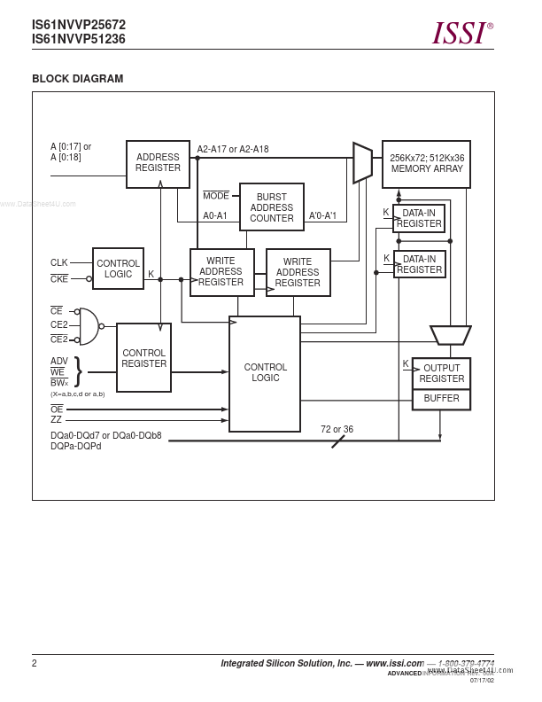
256K x 72 and 512K x 36, 18Mb PIPELINE 'NO WAIT' STATE BUS SRAM FEATURES • 100 percent bus utilization • No wait cycles between Read and Write • Internal self-timed write cycle www.DataSheet4U.com • Individual ISSI ADVANCE INFORMATION JULY 2002 DESCRIPTION ® Byte Write Control 
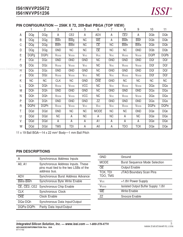
• Single R/W (Read/Write) control pin • Clock controlled, registered address, data and control • Interleaved or linear burst sequence control using MODE input • Power Down mode • Common data inputs and data outputs • CKE pin to enable clock and suspend operation • JEDEC 119-ball PBGA (x36) and 209-ball (x72) PBGA packages • Single +1.
Published: |