Datasheet4U Logo Datasheet4U.com

IDT71V35761S - 3.3V Synchronous SRAMs

Download the IDT71V35761S datasheet PDF (IDT71V35761SA included). The manufacturer datasheet provides complete specifications, pinout details, electrical characteristics, and typical applications for 3.3v synchronous srams.

Features

  • 128K x 36 memory configurations.
  • Supports high system speed: Commercial:.
  • 200MHz 3.1ns clock access time Commercial and Industrial:.
  • 183MHz 3.3ns clock access time.
  • 166MHz 3.5ns clock access time.
  • LBO input selects interleaved or linear burst mode.
  • 3.3V core power supply Functional Block Diagram LBO ADV CLK ADSC ADSP.
  • Self-timed write cycle with global write control (GW), byte write enable (BWE), and byte writes (BWx).
  • Power down control.

📥 Download Datasheet

Note: The manufacturer provides a single datasheet file (IDT71V35761SA-IDT.pdf) that lists specifications for multiple related part numbers.

Datasheet Details

Part number IDT71V35761S
Manufacturer IDT
File Size 818.92 KB
Description 3.3V Synchronous SRAMs
Datasheet download datasheet IDT71V35761S Datasheet
Other Datasheets by IDT

Full PDF Text Transcription

Click to expand full text
128K x 36 3.3V Synchronous SRAMs IDT71V35761S/SA 3.3V I/O, Pipelined Outputs Burst Counter, Single Cycle Deselect
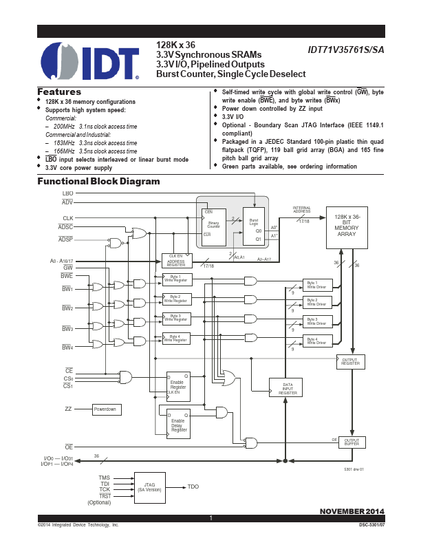
 Features ◆ 128K x 36 memory configurations ◆ Supports high system speed: Commercial: – 200MHz 3.1ns clock access time Commercial and Industrial: – 183MHz 3.3ns clock access time – 166MHz 3.5ns clock access time ◆ LBO input selects interleaved or linear burst mode ◆ 3.3V core power supply Functional Block Diagram LBO ADV CLK ADSC ADSP ◆ Self-timed write cycle with global write control (GW), byte write enable (BWE), and byte writes (BWx) ◆ Power down controlled by ZZ input ◆ 3.3V I/O ◆ Optional - Boundary Scan JTAG Interface (IEEE 1149.
Published: |