Click to expand full text
www.DataSheet4U.com
HY5DU283222Q
128M(4Mx32) GDDR SDRAM
HY5DU283222Q
This document is a general product description and is subject to change without notice. Hynix Electronics does not assume any responsibility for use of circuits described. No patent licenses are implied. Rev. 1.2/Oct. 02 1
HY5DU283222Q
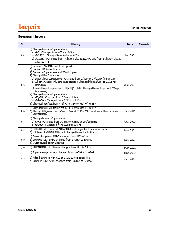
Revision History
No. History 1) Changed some AC parameters a) tAC : Changed from 0.7ns to 0.9ns b) tDQSCK : Changed from 0.6ns to 0.7ns c) tRCD/tRP : Changed from 4clks to 5clks at 222MHz and from 3clks to 4clks at 200/183MHz 1) 2) 3) 4) 0.5 Removed 166MHz part from speed bin Defined IDD specification Defined AC parameters of 250MHz part Changed Pin Capacitance a) Input Clock capacitance : Changed from 2/3pF to 1.7/2.
 HY5DU283222Q Datasheet