4 V gate drive device can be driven from 5 V source
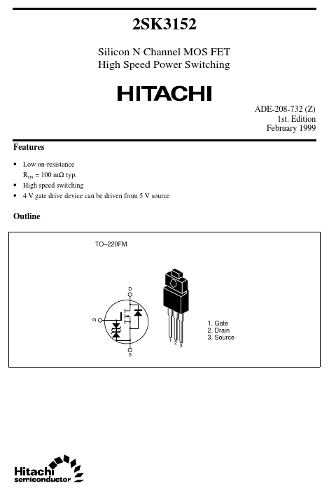
Outline
TO.
220FM
D
G
1 2 S
1. Gate 2. Drain 3. Source
3
2SK3152
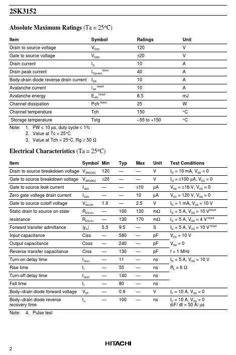
Absolute Maximum Ratings (Ta = 25°C)
Item Drain to source voltage Gate to source voltage Drain current Drain peak current Body-drain diode reverse drain current Avalanche current Avalanche energy Channel dissipation Channel temperature Storage temperature Note: Symbol VDSS VGSS ID.
Note: Below is a high-fidelity text extraction (approx. 800 characters) for
K3152. For precise diagrams, and layout, please refer to the original PDF.
2SK3152 Silicon N Channel MOS FET High Speed Power Switching ADE-208-732 (Z) 1st. Edition February 1999 Features • Low on-resistance R DS = 100 mΩ typ. • High speed switc...
View more extracted text
999 Features • Low on-resistance R DS = 100 mΩ typ. • High speed switching • 4 V gate drive device can be driven from 5 V source Outline TO–220FM D G 1 2 S 1. Gate 2. Drain 3. Source 3 2SK3152 Absolute Maximum Ratings (Ta = 25°C) Item Drain to source voltage Gate to source voltage Drain current Drain peak current Body-drain diode reverse drain current Avalanche current Avalanche energy Channel dissipation Channel temperature Storage temperature Note: Symbol VDSS VGSS ID I D(pulse) I DR I AP Note3 Note3 Note2 Note1 Ratings 120 ±20 10 40 10 10 8.5 25 150 –55 to +150 Unit V V A A A A mJ W °C °C EAR Pch Tch Tstg 1. PW ≤ 10 µs,
More Datasheets from Hitachi Semiconductor (now Renesas)
 K3152 Datasheet