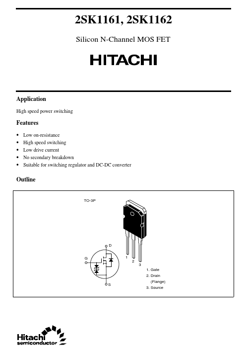
Suitable for switching regulator and DC-DC converter
Outline
TO-3P
D G1
2 3 1. Gate 2. Drain (Flange)
S 3. Source
2SK1161, 2SK1162
Absolute Maximum Ratings (Ta = 25°C)
Item
Drain to source voltage
2SK1161
2SK1162
Gate to source voltage
Drain current
Drain peak current
Body to drain diode reverse drain current
Channel dissipation
Channel temperature
Storag.
Note: Below is a high-fidelity text extraction (approx. 800 characters) for
K1162. For precise diagrams, and layout, please refer to the original PDF.
2SK1161, 2SK1162 Silicon N-Channel MOS FET Application High speed power switching Features • Low on-resistance • High speed switching • Low drive current • No secondary b...
View more extracted text
resistance • High speed switching • Low drive current • No secondary breakdown • Suitable for switching regulator and DC-DC converter Outline TO-3P D G1 2 3 1. Gate 2. Drain (Flange) S 3. Source 2SK1161, 2SK1162 Absolute Maximum Ratings (Ta = 25°C) Item Drain to source voltage 2SK1161 2SK1162 Gate to source voltage Drain current Drain peak current Body to drain diode reverse drain current Channel dissipation Channel temperature Storage temperature Notes: 1. PW ≤ 10 µs, duty cycle ≤ 1% 2.
More Datasheets from Hitachi Semiconductor (now Renesas)
 K1162 Datasheet