Click to expand full text
HD74ALVCH162501
18-bit Universal Bus Transceivers with 3-state Outputs
ADE-205-182 (Z) Preliminary 1st. Edition December 1996 Description
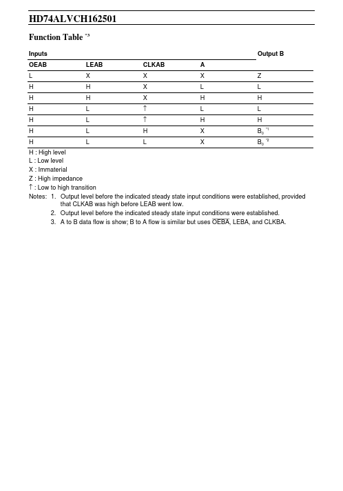
Data flow in each direction is controlled by output enable (OEAB and OEBA), latch enable (LEAB and LEBA), and clock (CLKAB and CLKBA) inputs. For A to B data flow, the device operates in the transparent mode when LEAB is high. When LEAB is low, the A data is latched if CLKAB is held at a high or low logic level. If LEAB is low, the A bus data is stored in the latch flip flop on the low to high transition of CLKAB. When OEAB is high, the outputs are active. When OEAB is low, the outputs are in the high impedance state. Data flow for B to A is similar to that of A to B but uses OEBA , LEBA, and CLKBA.
 HD74ALVCH162501 Datasheet