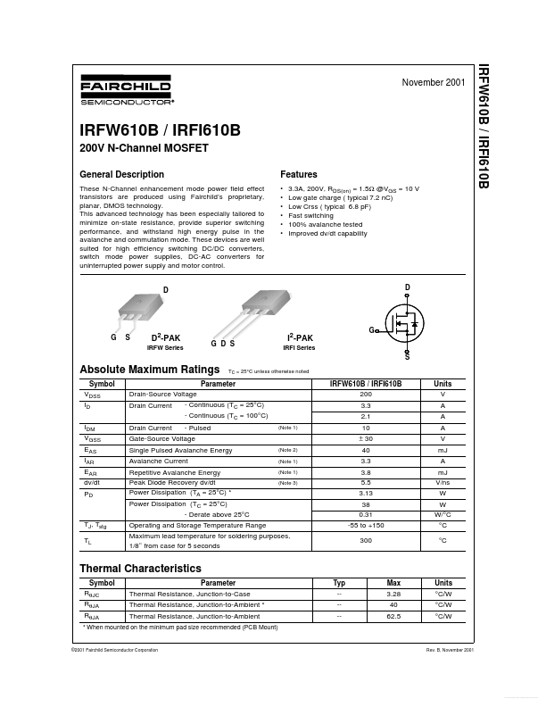
These N-Channel enhancement mode power field effect transistors are produced using Fairchild’s proprietary, planar, DMOS technology.
Key Features
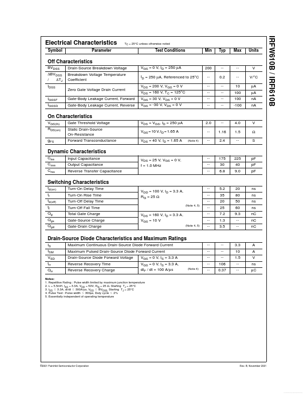
3.3A, 200V, RDS(on) = 1.5Ω @VGS = 10 V Low gate charge ( typical 7.2 nC) Low Crss ( typical 6.8 pF) Fast switching 100% avalanche tested Improved dv/dt capability
D
D
!.
◀
▲.
G
S
D2-PAK
IRFW Series
G D S
I2-PAK
IRFI Series
G!
!
S
Absolute Maximum Ratings
Symbol VDSS ID IDM VGSS EAS IAR EAR dv/dt PD
TC = 25°C unless otherwise noted
Parameter Drain-Source Voltage - Continuous (TC = 25°C) Drain Current - Cont.
Full PDF Text Transcription for IRFW610B (Reference)
Note: Below is a high-fidelity text extraction (approx. 800 characters) for
IRFW610B. For precise diagrams, and layout, please refer to the original PDF.
IRFW610B / IRFI610B November 2001 IRFW610B / IRFI610B 200V N-Channel MOSFET General Description These N-Channel enhancement mode power field effect transistors are produc...
View more extracted text
e N-Channel enhancement mode power field effect transistors are produced using Fairchild’s proprietary, planar, DMOS technology. This advanced technology has been especially tailored to minimize on-state resistance, provide superior switching performance, and withstand high energy pulse in the avalanche and commutation mode. These devices are well suited for high efficiency switching DC/DC converters, switch mode power supplies, DC-AC converters for uninterrupted power supply and motor control. Features • • • • • • 3.3A, 200V, RDS(on) = 1.5Ω @VGS = 10 V Low gate charge ( typical 7.2 nC) Low Crss ( typical 6.
 IRFW610B Datasheet