FDMC6296 Datasheet Text
FDMC6296 N-Channel Power Trench® MOSFET
FDMC6296
Single N-Channel Logic-Level Power Trench® MOSFET
30 V, 11.5 A, 10.5 mΩ
Features
- Max rDS(on) = 10.5 mΩ at VGS = 10 V, ID = 11.5 A
- Max rDS(on) = 15 mΩ at VGS = 4.5 V, ID = 10 A
- Low Qg, Qgd and Rg for efficient switching performance
- RoHS pliant
November 2010
General Description
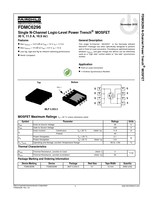
This single N-Channel MOSFET in the thermally efficient MicroFET Package has been specifically designed to perform well in Point of Load converters. Providing an optimized balance between rDS(on) and gate charge this device can be effectively used as a “high side” control swtich or “low side” synchronous rectifier.
Application
- Point of Load Converters
- 1/16 Brick Synchronous Rectifier
Top Pin 1 S S S G
Bottom D D D D D D D D 8 1 S 5 6 7 4 3 2 G S S
MLP 3.3X3.3
MOSFET Maximum Ratings TA = 25 °C unless otherwise noted
Symbol VDS VGS ID PD TJ, TSTG Parameter Drain to Source Voltage Gate to Source Voltage Drain Current Power Dissipation Power Dissipation -Continuous -Pulsed TC = 25 °C TA = 25 °C (Note 1a) TA = 25 °C (Note 1a) Ratings 30 ±20 11.5 40 2.1 0.9 -55 to +150 W °C Units V V A
Operating and Storage Junction Temperature Range
Thermal Characteristics
RθJC RθJA Thermal Resistance, Junction to Case Thermal Resistance, Junction to Ambient (Note 1) (Note 1a) 3 53 °C/W
Package Marking and Ordering Information
Device Marking FDMC6296 Device FDMC6296 Package MLP 3.3X3.3 Reel Size 13 ’’ Tape Width 12 mm Quantity 3000 units
©2010 Fairchild Semiconductor Corporation FDMC6296 Rev. C2
1
.fairchildsemi. http://..
FDMC6296 N-Channel Power Trench® MOSFET
Electrical Characteristics TJ = 25 °C unless otherwise noted...