Download FDMC6675BZ Datasheet PDF
FDMC6675BZ page 2
Page 2
FDMC6675BZ page 3
Page 3

FDMC6675BZ Datasheet Text

FDMC6675BZ P-Channel PowerTrench® MOSFET FDMC6675BZ P-Channel Power Trench® MOSFET -30 V, -20 A, 14.4 mΩ Features - Max rDS(on) = 14.4 mΩ at VGS = -10 V, ID = -9.5 A - Max rDS(on) = 27.0 mΩ at VGS = -4.5 V, ID = -6.9 A - HBM ESD protection level of 8 kV typical(note 3) - Extended VGSS range (-25 V) for battery applications - High performance trench technology for extremely low rDS(on) - High power and current handling capability - Termination is Lead-free and RoHS pliant June 2009 General Description 
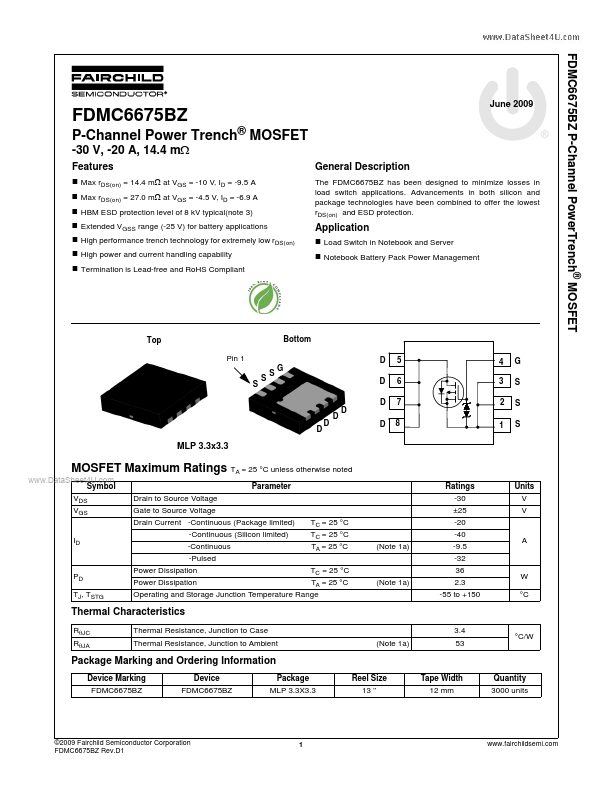
The FDMC6675BZ has been designed to minimize losses in load switch applications. Advancements in both silicon and package technologies have been bined to offer the lowest rDS(on) and ESD protection. Application - Load Switch in Notebook and Server - Notebook Battery Pack Power Management Top Pin 1 S S S G Bottom D D D D D D D D 8 1 5 6 7 4 3 2 G S S S MLP 3.3x3.3 MOSFET Maximum Ratings TA = 25 °C unless otherwise noted .. Symbol VDS VGS Parameter Drain to Source Voltage Gate to Source Voltage Drain Current -Continuous (Package limited) ID -Continuous (Silicon limited) -Continuous -Pulsed PD TJ, TSTG Power Dissipation Power Dissipation TC = 25 °C TA = 25 °C (Note 1a) TC = 25 °C TC = 25 °C TA = 25 °C (Note 1a) Ratings -30 ±25 -20 -40 -9.5 -32 36 2.3 -55 to +150 W °C A Units V V Operating and Storage Junction Temperature Range Thermal Characteristics RθJC RθJA Thermal Resistance, Junction to Case Thermal Resistance, Junction to Ambient (Note 1a) 3.4 53 °C/W Package Marking and Ordering Information Device Marking FDMC6675BZ Device FDMC6675BZ Package MLP 3.3X3.3 Reel Size 13 ’’ Tape Width 12 mm Quantity 3000 units ©2009 Fairchild Semiconductor Corporation FDMC6675BZ Rev.D1...