Click to expand full text
www.DataSheet4U.com
xr
FEBRUARY 2006
PRELIMINARY
XRK39653
REV. P1.0.0
3.3V, 8-OUTPUT ZERO DELAY BUFFER
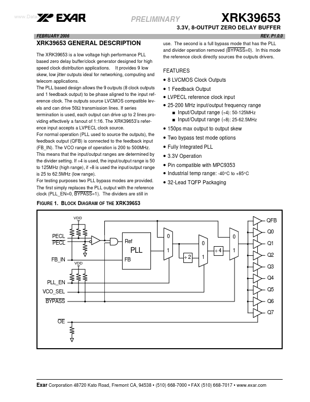
use. The second is a full bypass mode that has the PLL and divider operation removed (BYPASS=0). In this mode the reference clock directly sources the outputs drivers.
XRK39653 GENERAL DESCRIPTION
The XRK39653 is a low voltage high performance PLL based zero delay buffer/clock generator designed for high speed clock distribution applications. It provides 9 low skew, low jitter outputs ideal for networking, computing and telecom applications. The PLL based design allows the 9 outputs (8 clock outputs and 1 feedback output) to be phase aligned to the input reference clock. The outputs source LVCMOS compatible levels and can drive 50Ω transmission lines.
 XRK39653 Datasheet