Click to expand full text
www.DataSheet4U.com
MAY 2006
PRELIMINARY
XRK32309
REV. P1.0.1
LOW-COST 3.3V ZERO DELAY BUFFER
GENERAL DESCRIPTION
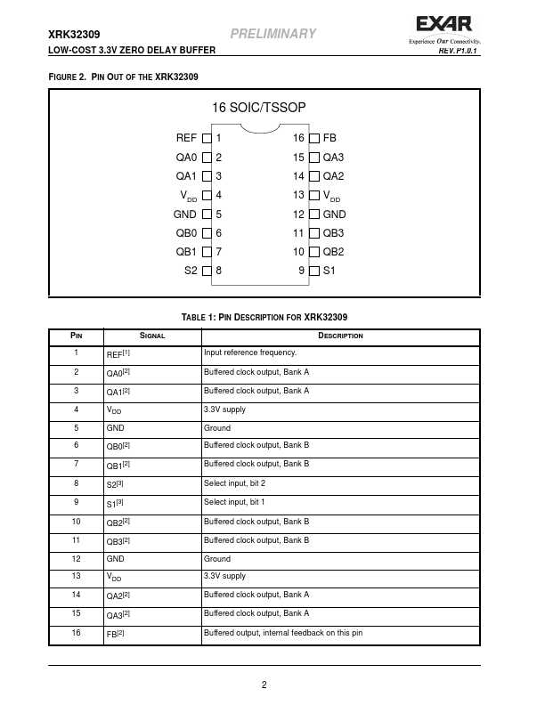
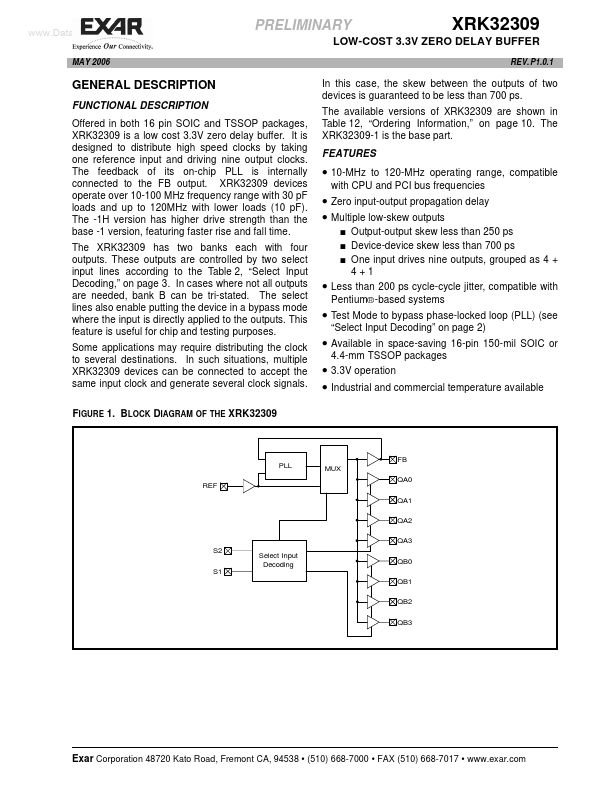
FUNCTIONAL DESCRIPTION Offered in both 16 pin SOIC and TSSOP packages, XRK32309 is a low cost 3.3V zero delay buffer. It is designed to distribute high speed clocks by taking one reference input and driving nine output clocks. The feedback of its on-chip PLL is internally connected to the FB output. XRK32309 devices operate over 10-100 MHz frequency range with 30 pF loads and up to 120MHz with lower loads (10 pF). The -1H version has higher drive strength than the base -1 version, featuring faster rise and fall time. The XRK32309 has two banks each with four outputs.
 XRK32309 Datasheet