Click to expand full text
58
PRELIMINARY
CY28358
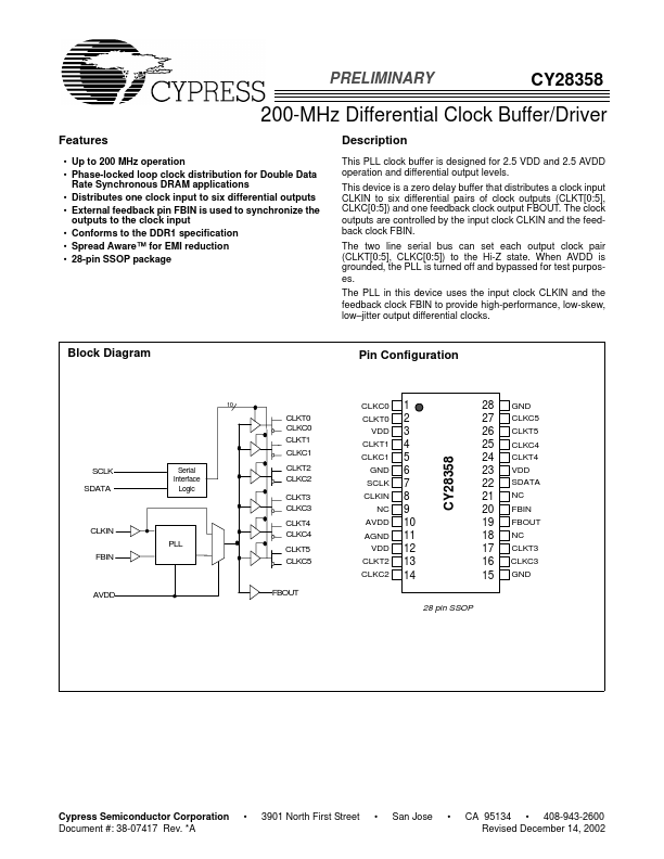
200-MHz Differential Clock Buffer/Driver
Features
• Up to 200 MHz operation • Phase-locked loop clock distribution for Double Data Rate Synchronous DRAM applications • Distributes one clock input to six differential outputs • External feedback pin FBIN is used to synchronize the outputs to the clock input • Conforms to the DDR1 specification • Spread Aware™ for EMI reduction • 28-pin SSOP package
Description
This PLL clock buffer is designed for 2.5 VDD and 2.5 AVDD operation and differential output levels. This device is a zero delay buffer that distributes a clock input CLKIN to six differential pairs of clock outputs (CLKT[0:5], CLKC[0:5]) and one feedback clock output FBOUT.
 CY28358 Datasheet