Click to expand full text
CY28352
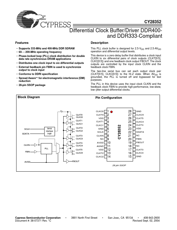
Differential Clock Buffer/Driver DDR400and DDR333-Compliant
Features
• Supports 333-MHz and 400-MHz DDR SDRAM • 60- – 200-MHz operating frequency • Phase-locked loop (PLL) clock distribution for double data rate synchronous DRAM applications • Distributes one clock input to six differential outputs • External feedback pin FBIN is used to synchronize output to clock input • Conforms to DDRI specification • Spread Aware™ for electromagnetic interference (EMI) reduction • 28-pin SSOP package
Description
This PLL clock buffer is designed for 2.5-VDD and 2.5-AVDD operation and differential output levels. This device is a zero delay buffer that distributes a clock input CLKIN to six differential pairs of clock outputs (CLKT[0:5], CLKC[0:5]) and one feedback clock output FBOUT.
 CY28352 Datasheet