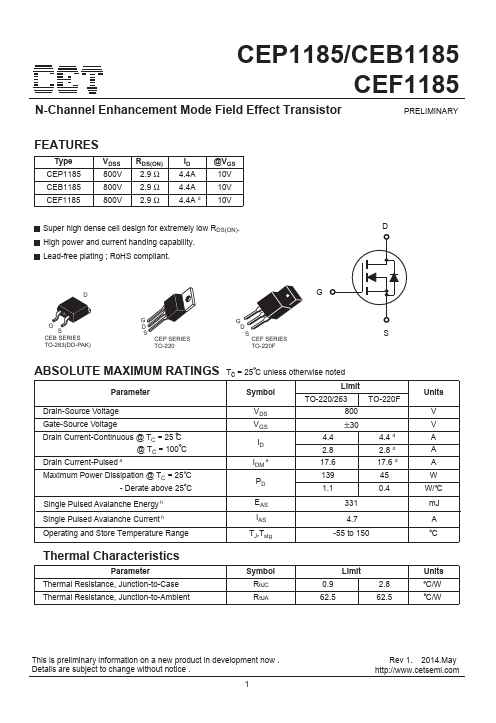
Type CEP1185 CEB1185 CEF1185
VDSS 800V 800V
800V
RDS(ON) 2.9 Ω 2.9 Ω
2.9 Ω
ID 4.4A 4.4A 4.4A d
@VGS 10V 10V
10V
Super high dense cell design for extremely low RDS(ON). High power and current handing capability. Lead-free plating ; RoHS compliant. D
DG
GS
CEB SERIES TO-263(DD-PAK)
G D S
CEP SERIES TO-220
G
D S CEF SERIES
TO-220F
S.
N-Channel Enhancement Mode Field Effect Transistor
Full PDF Text Transcription (Reference)
The following content is an automatically extracted verbatim text
from the original manufacturer datasheet and is provided for reference purposes only.
View original datasheet text
CEP1185/CEB1185
CEF1185
N-Channel Enhancement Mode Field Effect Transistor
PRELIMINARY
FEATURES
Type CEP1185 CEB1185 CEF1185
VDSS 800V 800V
800V
RDS(ON) 2.9 Ω 2.9 Ω
2.9 Ω
ID 4.4A 4.4A 4.4A d
@VGS 10V 10V
10V
Super high dense cell design for extremely low RDS(ON). High power and current handing capability. Lead-free plating ; RoHS compliant.
D
DG
GS
CEB SERIES TO-263(DD-PAK)
G D S
CEP SERIES TO-220
G
D S CEF SERIES
TO-220F
S
ABSOLUTE MAXIMUM RATINGS
Parameter
Drain-Source Voltage Gate-Source Voltage Drain Current-Continuous @ TC = 25 C
@ TC = 100 C Drain Current-Pulsed a Maximum Power Dissipation @ TC = 25 C
- Derate above 25 C
Tc = 25 C unless otherwise noted
Symbol
Limit TO-220/263
VDS 800
VGS ±30
ID
4.4 2.8
IDM e
17.6
139 PD 1.1
TO-220F
4.4 d 2.8 d 17.6 d 45 0.
 CEB1185 Datasheet