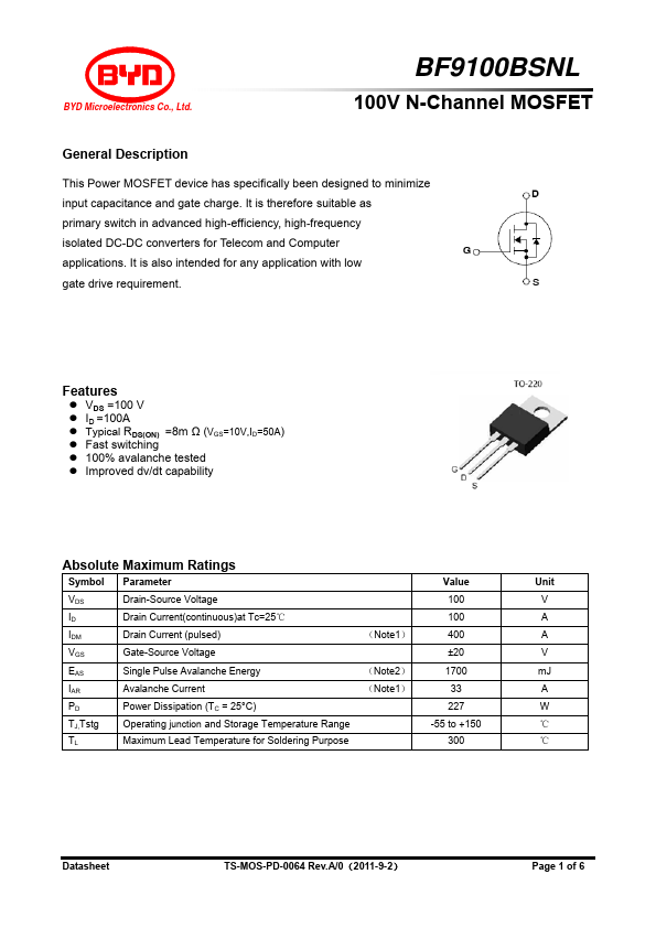
Description
This Power MOSFET device has specifically been designed to minimize input capacitance and gate charge.
It is therefore suitable as primary switch in advanced high-efficiency, high-frequency isolated DC-DC converters for Telecom and Computer applications.
Features
- z VDS =100 V z ID =100A z Typical RDS(ON) =8m Ω (VGS=10V,ID=50A) z Fast switching z 100% avalanche tested z Improved dv/dt capability
Absolute Maximum Ratings
Symbol Parameter
VDS Drain-Source Voltage
ID Drain Current(continuous)at Tc=25℃
IDM Drain Current (pulsed)
VGS Gate-Source Voltage
EAS Single Pulse Avalanche Energy
IAR Avalanche Current
PD Power Dissipation (TC = 25°C)
TJ,Tstg TL
Operating junction and Storage Temperature Range Maximum Lead Temperature for Soldering Purpose
(N.
 BF9100BSNL Datasheet