Datasheet Details
| Part number | AON6156 |
|---|---|
| Manufacturer | Alpha & Omega Semiconductors |
| File Size | 313.76 KB |
| Description | 45V N-Channel MOSFET |
| Datasheet |
 AON6156 Datasheet AON6156 Datasheet
|
|
|
| Part number | AON6156 |
|---|---|
| Manufacturer | Alpha & Omega Semiconductors |
| File Size | 313.76 KB |
| Description | 45V N-Channel MOSFET |
| Datasheet |
AON6156 Datasheet
|
|
|
|
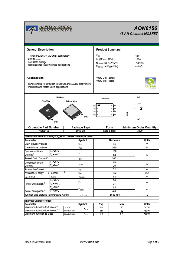
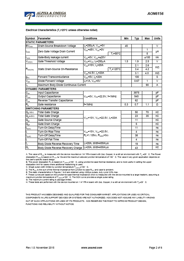
• Trench Power MV MOSFET technology • Low RDS(ON) • Low Gate Charge • Optimized for fast-switching applications Product Summary VDS ID (at VGS=10V) RDS(ON) (at VGS=10V) RDS(ON) (at VGS=4.5V) 45V 100A < 2.6mΩ < 4mΩ Applications • Synchronous Rectification in DC/DC and AC/DC Converters • Industrial and Motor Drive applications 100% UIS Tested 100% Rg Tested Top View DFN5x6 Bottom View PIN1 PIN1 Top View 1 8 2 7 3 6 4 5 D G S Orderable Part Number AON6156 Package Type DFN 5x6 Form Tape & Reel Minimum Order Quantity 3000 Absolute Maximum Ratings TA=25°C unless otherwise noted Parameter Symbol Drain-Source Voltage VDS Gate-Source Voltage VGS Continuous Drain Current G TC=25°C TC=100°C ID Pulsed Drain Current C IDM Continuous Drain Current TA=25°C TA=70°C IDSM Avalanche Current C IAS Avalanche energy L=0.3mH C EAS VDS Spike Power Dissipation B 10µs TC=25°C TC=100°C VSPIKE PD Power Dissipation A TA=25°C TA=70°C PDSM Junction and Storage Temperature Range TJ, TSTG Maximum 45 ±20 100 82 260 36 29 32 154 54 78 31 6.2 4.0 -55 to 150 Units V V A A A mJ V W W °C Thermal Characteristics Parameter Symbol Typ Maximum Junction-to-Ambient A Maximum Junction-to-Ambient A D t ≤ 10s Steady-State RθJA 15 40 Maximum Junction-to-Case Steady-State RθJC 1.3 Max 20 50 1.6 Units °C/W °C/W °C/W Rev.1.0: November 2015 www.aosmd.com Page 1 of 6 AON6156 Electrical Characteristics (TJ=25°C unless otherwise noted) Symbol Parameter Conditions Min STATIC PARAMETERS BVDSS Drain-Source Breakdown Voltage ID=250µA, VGS=0V 45 IDSS Zero Gate Voltage Drain Current VDS=45V, VGS=0V TJ=55°C IGSS Gate-Body leakage current VDS=0V, VGS=±20V VGS(th) Gate Threshold Voltage VDS=VGS, ID=250µA 1.5 VGS=10V, ID=20A RDS(ON) Static Drain-Source On-Resistance TJ=125°C VGS=4.5V, ID=20A gFS Forward Transconductance VDS=5V, ID=20A VSD Diode Forward Voltage IS=1A, VGS=0V IS Maximu
AON6156 45V N-Channel MOSFET General.
| Part Number | Description |
|---|---|
| AON6152A | 45V N-Channel MOSFET |
| AON6154 | 45V N-Channel MOSFET |
| AON6144 | 40V N-Channel MOSFET |
| AON6160 | N-Channel MOSFET |
| AON6162 | 60V N-Channel MOSFET |
| AON6200 | 30V N-Channel MOSFET |
| AON6202 | 30V N-Channel MOSFET |
| AON6204 | 30V N-Channel MOSFET |
| AON6206 | 30V N-Channel MOSFET |
| AON6210 | 30V N-Channel MOSFET |